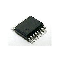
CM2009-00QR ON Semiconductor, CM2009-00QR Datasheet - Page 6

CM2009-00QR
Manufacturer Part Number
CM2009-00QR
Description
VGA PORT COMPANION-65 OHM QSOP16
Manufacturer
ON Semiconductor
Type
The CM2009 connects between a video graphics controller embedded in a PC, graphics adapter card or set top box and the VGA or DVI-I port connector.r
Datasheet
1.CM2009-00QR.pdf
(8 pages)
Specifications of CM2009-00QR
Voltage - Working
6V
Voltage - Clamping
6V
Technology
Diode Array
Power (watts)
500mW
Number Of Circuits
1
Applications
General Purpose
Package / Case
16-QSOP
Operating Supply Voltage
- 0.5 V to + 6 V
Supply Current
10 uA
Maximum Operating Temperature
+ 85 C
Minimum Operating Temperature
- 40 C
Mounting Style
SMD/SMT
Number Of Channels
7
Operating Temperature (min)
-40C
Operating Temperature Classification
Industrial
Operating Temperature (max)
85C
Package Type
QSOP
Rad Hardened
No
Lead Free Status / RoHS Status
Lead free / RoHS Compliant
Available stocks
Company
Part Number
Manufacturer
Quantity
Price
Part Number:
CM2009-00QR
Manufacturer:
CMD
Quantity:
20 000
Application Information
NOTES
1
2
3
4
5
6
7
8
9
10 R1, R2 are optional. They may be used, if required, to pull the DDC_CLK and DDC_DATA lines to VCC_5V when no
11 For optimal ESD performance with the CM2009-02, an additional clamp device (such as the CMD PACDN042) should
The CM2009 should be placed as close to the VGA or DVI-I connector as possible.
The ESD protection channels VIDEO_1, VIDEO_2, VIDEO_3 may be used interchangeably between the R, G, B
signals.
If differential video signal routing is used, the RED, BLUE, and GREEN signal lines should be terminated with external
37.5 resistors.
"VF" are external video filters for the RGB signals.
Supply bypass capacitors C1 and C2 must be placed immediately adjacent to the corresponding Vcc pins. Connections
to the Vcc pins and ground plane must be made with minimal length copper traces (preferably less than 5mm) for best
ESD protection.
The bypass capacitor for the BYP pin has been omitted in this diagram. This results in a reduction in the maximum ESD
withstand voltage at the DDC_OUT pins from ±8kV to ±4kV. If 8kV ESD protection is required, a 0.2µF ceramic bypass
capacitor should be connected between BYP and ground.
The SYNC buffers may be used interchangeably between HSYNC and VSYNC.
The EMI filters at the SYNC_OUT and DDC_OUT pins (C5 to C12, and Ferrite Beads FB1 to FB4) are for reference
only. The component values and filter configuration may be changed to suit the application.
The DDC level shifters DDC_IN, DDC_OUT, may be used interchangeably between DDCA_CLK and DDCA_DATA.
monitor is connected to the VGA connector. If used, it should be noted that "back current" may flow between the DDC
pins and VCC_5V via these resistors when VCC_5V is powered down.
be placed on HSYNC/VSYNC lines between the external matching resistor and the VGA connector.
Figure 1. Typical Application Connection Diagram
Rev. 3 | Page 6 of 8 | www.onsemi.com
CM2009


