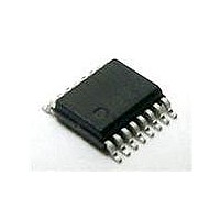
CM2009-00QR ON Semiconductor, CM2009-00QR Datasheet - Page 5

CM2009-00QR
Manufacturer Part Number
CM2009-00QR
Description
VGA PORT COMPANION-65 OHM QSOP16
Manufacturer
ON Semiconductor
Type
The CM2009 connects between a video graphics controller embedded in a PC, graphics adapter card or set top box and the VGA or DVI-I port connector.r
Datasheet
1.CM2009-00QR.pdf
(8 pages)
Specifications of CM2009-00QR
Voltage - Working
6V
Voltage - Clamping
6V
Technology
Diode Array
Power (watts)
500mW
Number Of Circuits
1
Applications
General Purpose
Package / Case
16-QSOP
Operating Supply Voltage
- 0.5 V to + 6 V
Supply Current
10 uA
Maximum Operating Temperature
+ 85 C
Minimum Operating Temperature
- 40 C
Mounting Style
SMD/SMT
Number Of Channels
7
Operating Temperature (min)
-40C
Operating Temperature Classification
Industrial
Operating Temperature (max)
85C
Package Type
QSOP
Rad Hardened
No
Lead Free Status / RoHS Status
Lead free / RoHS Compliant
Available stocks
Company
Part Number
Manufacturer
Quantity
Price
Part Number:
CM2009-00QR
Manufacturer:
CMD
Quantity:
20 000
CM2009
SYMBOL PARAMETER
C
V
t
V
I
t
t
IN_VID
R,
I
OFF
PLH
PHL
ESD
IN
ON
t
F
Note 1: All parameters specified over standard operating conditions unless otherwise noted.
Note 2: These parameters apply only to the SYNC drivers. Note that R
Note 3: Per the IEC-61000-4-2 International ESD Standard, Level 4 contact discharge method. BYP, V
Note 4: The SYNC_OUT pins on the CM2009-02 are guaranteed for 2kV HBM ESD protection.
Input Current
Level Shifting N-MOSFET "OFF" State
Leakage Current
Voltage Drop Across Level-shifting
N-MOSFET when "ON"
VIDEO Input Capacitance
SYNC Driver L => H Propagation Delay
SYNC Driver H => L Propagation Delay
SYNC Driver Output Rise & Fall Times
ESD Withstand Voltage
VIDEO Inputs
SYNC_IN1, SYNC_IN2 Inputs
bypassed to GND via a low impedance ground plane with a 0.2µF, low inductance, chip ceramic capacitor at each supply
pin. ESD pulse is applied between the applicable pins and GND. ESD pulses can be positive or negative with respect to
GND. Applicable pins are: VIDEO_1, VIDEO_2, VIDEO_3, SYNC_OUT1, SYNC_OUT2, DDC_OUT1 and DDC_OUT2.
All other pins are ESD protected to the industry standard 2kV Human Body Model (MIL-STD-883, Method 3015). The
bypass capacitor at the BYP pin may optionally be omitted, in which case the max. ESD withstand voltage for the
DDC_OUT1 and DDC_OUT2 pins are reduced to ±4kV.
Rev. 3 | Page 5 of 8 | www.onsemi.com
CONDITIONS
V
V
(V
(V
V
V
V
C
C
C
V
CC_VIDEO
CC_SYNC
CC_DDC
CC_VIDEO
CC_VIDEO
CC_VIDEO
L
L
L
CC_DDC
CC_DDC
= 50pF; V
= 50pF; V
= 50pF; V
= 2.5V; V
- V
- V
= 5.0V; V
= 5.0V; V
= 5.0V; V
= 2.5V; V
= V
DDC_IN
DDC_OUT
CC_SYNC
CC
CC
CC
) ≤ 0.4V; V
= 5.0V; Input t
= 5.0V; Input t
= 5.0V; Input t
) ≤ 0.4V; V
S
IN
IN
IN
IN
= 5V; Notes 3, 4 & 5
= GND; I
= V
= V
= 2.5V; ƒ = 1MHz; Note 4
= 1.25V; ƒ = 1MHz; Note 4
CC_SYNC
OUT
CC_VIDEO
= R
DDC_OUT
DDC_IN
DS
or GND
T
or GND
= 3mA;
R
R
R
+ R
and t
and t
and t
= V
= V
BUFFER
CC_DDC
CC_DDC
F
F
F
≤ 5ns
≤ 5ns
≤ 5ns
.
MIN
CC_VIDEO
±8
TYP
and V
4
CC_SYNC
MAX UNITS
0.18
4.5
10
10
12
12
±1
±1
4
must be
µA
µA
µA
µA
kV
pF
pF
ns
ns
ns
V


