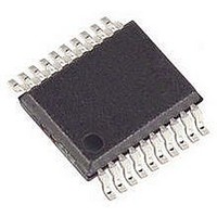
PIC16F1828-I/SS Microchip Technology, PIC16F1828-I/SS Datasheet - Page 283

PIC16F1828-I/SS
Manufacturer Part Number
PIC16F1828-I/SS
Description
IC PIC MCU 8BIT 14KB FLSH 20SSOP
Manufacturer
Microchip Technology
Series
PIC® XLP™ 16Fr
Datasheets
1.PIC16F722-ISS.pdf
(8 pages)
2.PIC16F1826-IP.pdf
(40 pages)
3.PIC16F1824-ISL.pdf
(2 pages)
4.PIC16F1824-ISL.pdf
(419 pages)
5.PIC16F1824-ISL.pdf
(10 pages)
Specifications of PIC16F1828-I/SS
Core Size
8-Bit
Program Memory Size
7KB (4K x 14)
Core Processor
PIC
Speed
32MHz
Connectivity
I²C, SPI, UART/USART
Peripherals
Brown-out Detect/Reset, POR, PWM, WDT
Number Of I /o
17
Program Memory Type
FLASH
Eeprom Size
256 x 8
Ram Size
256 x 8
Voltage - Supply (vcc/vdd)
1.8 V ~ 5.5 V
Data Converters
A/D 12x10b
Oscillator Type
Internal
Operating Temperature
-40°C ~ 85°C
Package / Case
20-SSOP (0.200", 5.30mm Width)
Controller Family/series
PIC16F
No. Of I/o's
18
Eeprom Memory Size
256Byte
Ram Memory Size
256Byte
Cpu Speed
32MHz
No. Of Timers
5
Lead Free Status / RoHS Status
Lead free / RoHS Compliant
Available stocks
Company
Part Number
Manufacturer
Quantity
Price
Part Number:
PIC16F1828-I/SS
Manufacturer:
MIC
Quantity:
20 000
- PIC16F722-ISS PDF datasheet
- PIC16F1826-IP PDF datasheet #2
- PIC16F1824-ISL PDF datasheet #3
- PIC16F1824-ISL PDF datasheet #4
- PIC16F1824-ISL PDF datasheet #5
- Current page: 283 of 419
- Download datasheet (4Mb)
25.6.8
An Acknowledge sequence is enabled by setting the
Acknowledge Sequence Enable bit, ACKEN bit of the
SSP1CON2 register. When this bit is set, the SCL pin is
pulled low and the contents of the Acknowledge data bit
are presented on the SDA pin. If the user wishes to gen-
erate an Acknowledge, then the ACKDT bit should be
cleared. If not, the user should set the ACKDT bit before
starting an Acknowledge sequence. The Baud Rate
Generator then counts for one rollover period (T
and the SCL pin is deasserted (pulled high). When the
SCL pin is sampled high (clock arbitration), the Baud
Rate Generator counts for T
pulled low. Following this, the ACKEN bit is automatically
cleared, the Baud Rate Generator is turned off and the
MSSP1
(Figure
25.6.8.1
If the user writes the SSP1BUF when an Acknowledge
sequence is in progress, then the WCOL bit is set and
the contents of the buffer are unchanged (the write
doesn’t occur).
FIGURE 25-30:
2010 Microchip Technology Inc.
25-29).
module
Note: T
ACKNOWLEDGE SEQUENCE
TIMING
WCOL Status Flag
SSP1IF
BRG
Acknowledge sequence starts here,
SDA
SCL
then
= one Baud Rate Generator period.
ACKNOWLEDGE SEQUENCE WAVEFORM
SSP1IF set at
the end of receive
goes
BRG
ACKEN = 1, ACKDT = 0
. The SCL pin is then
write to SSP1CON2
into
Idle
8
D0
mode
BRG
Preliminary
)
Cleared in
software
T
BRG
ACK
25.6.9
A Stop bit is asserted on the SDA pin at the end of a
receive/transmit by setting the Stop Sequence Enable
bit, PEN bit of the SSP1CON2 register. At the end of a
receive/transmit, the SCL line is held low after the
falling edge of the ninth clock. When the PEN bit is set,
the master will assert the SDA line low. When the SDA
line is sampled low, the Baud Rate Generator is
reloaded and counts down to ‘0’. When the Baud Rate
Generator times out, the SCL pin will be brought high
and one T
later, the SDA pin will be deasserted. When the SDA
pin is sampled high while SCL is high, the P bit of the
SSP1STAT register is set. A T
cleared and the SSP1IF bit is set
25.6.9.1
If the user writes the SSP1BUF when a Stop sequence
is in progress, then the WCOL bit is set and the
contents of the buffer are unchanged (the write doesn’t
occur).
PIC16(L)F1824/1828
T
BRG
9
SSP1IF set at the end
of Acknowledge sequence
BRG
STOP CONDITION TIMING
WCOL Status Flag
ACKEN automatically cleared
(Baud Rate Generator rollover count)
Cleared in
software
BRG
(Figure
later, the PEN bit is
DS41419B-page 283
25-30).
Related parts for PIC16F1828-I/SS
Image
Part Number
Description
Manufacturer
Datasheet
Request
R

Part Number:
Description:
IC, 8BIT MCU, PIC16F, 32MHZ, SOIC-18
Manufacturer:
Microchip Technology
Datasheet:

Part Number:
Description:
IC, 8BIT MCU, PIC16F, 32MHZ, SSOP-20
Manufacturer:
Microchip Technology
Datasheet:

Part Number:
Description:
IC, 8BIT MCU, PIC16F, 32MHZ, DIP-18
Manufacturer:
Microchip Technology
Datasheet:

Part Number:
Description:
IC, 8BIT MCU, PIC16F, 32MHZ, QFN-28
Manufacturer:
Microchip Technology
Datasheet:

Part Number:
Description:
IC, 8BIT MCU, PIC16F, 32MHZ, QFN-28
Manufacturer:
Microchip Technology
Datasheet:

Part Number:
Description:
IC, 8BIT MCU, PIC16F, 32MHZ, QFN-28
Manufacturer:
Microchip Technology
Datasheet:

Part Number:
Description:
IC, 8BIT MCU, PIC16F, 32MHZ, SSOP-20
Manufacturer:
Microchip Technology
Datasheet:

Part Number:
Description:
IC, 8BIT MCU, PIC16F, 20MHZ, DIP-40
Manufacturer:
Microchip Technology
Datasheet:

Part Number:
Description:
IC, 8BIT MCU, PIC16F, 32MHZ, QFN-28
Manufacturer:
Microchip Technology
Datasheet:

Part Number:
Description:
IC, 8BIT MCU, PIC16F, 20MHZ, MQFP-44
Manufacturer:
Microchip Technology
Datasheet:

Part Number:
Description:
IC, 8BIT MCU, PIC16F, 20MHZ, QFN-20
Manufacturer:
Microchip Technology
Datasheet:

Part Number:
Description:
IC, 8BIT MCU, PIC16F, 32MHZ, QFN-28
Manufacturer:
Microchip Technology
Datasheet:

Part Number:
Description:
MCU 14KB FLASH 768B RAM 64-TQFP
Manufacturer:
Microchip Technology
Datasheet:

Part Number:
Description:
7 KB Flash, 384 Bytes RAM, 32 MHz Int. Osc, 16 I/0, Enhanced Mid Range Core, Low
Manufacturer:
Microchip Technology

Part Number:
Description:
14KB Flash, 512B RAM, 256B EEPROM, LCD, 1.8-5.5V 40 UQFN 5x5x0.5mm TUBE
Manufacturer:
Microchip Technology
Datasheet:


