STE50DE100 STMicroelectronics, STE50DE100 Datasheet
STE50DE100
Specifications of STE50DE100
Available stocks


Related parts for STE50DE100


STE50DE100 Summary of contents
Page 1
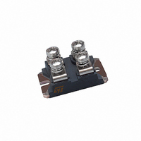
... Welding Description The STE50DE100 is manufactured in a hybrid structure, using dedicated high voltage Bipolar and low voltage MOSFET technologies, aimed to providing the best performance in ESBT topology. The STE50DE100 is designed for use in industrial converters and/or welding equipment. Order codes Part Number Marking STE50DE100 ...
Page 2
... Contents 1 Electrical ratings . . . . . . . . . . . . . . . . . . . . . . . . . . . . . . . . . . . . . . . . . . . . 3 2 Electrical characteristics . . . . . . . . . . . . . . . . . . . . . . . . . . . . . . . . . . . . . 4 2.1 Electrical characteristics (curves) 2.2 Test circuits . . . . . . . . . . . . . . . . . . . . . . . . . . . . . . . . . . . . . . . . . . . . . . . . 7 3 Package mechanical data . . . . . . . . . . . . . . . . . . . . . . . . . . . . . . . . . . . . . 8 4 Revision history . . . . . . . . . . . . . . . . . . . . . . . . . . . . . . . . . . . . . . . . . . . 10 2/11 STE50DE100 . . . . . . . . . . . . . . . . . . . . . . . . . . . 5 ...
Page 3
... STE50DE100 Electrical ratings 1 Table 1. Absolute maximum rating Symbol V Collector-source voltage (V CS(SS) V Base-source voltage (I BS(OS) V Source-base voltage (I SB(OS) V Gate-source voltage GS I Collector current C I Collector peak current ( Base current B I Base peak current ( Total dissipation at T tot Insulation withstand voltage (AC-RMS) from all four leads ...
Page 4
... 800V Clamp µ 47Ω 300V V CC Clamp = R 47Ω 25A Bpeak 300V V CC Clamp = R 47Ω 25A Bpeak C STE50DE100 Min. Typ. Max. Unit = 50A I = 10A 1 30A 1 50A 30A 50A I = 10A 2 30A_ 1.4 B µ = 250 A 3 3.7 B 2500 = 10V 50A C = 10V GS 650 R = 47Ω ...
Page 5
... STE50DE100 2.1 Electrical characteristics (curves) Figure 1. Output characteristics Figure 3. Collector-source On voltage Figure 5. Base-source On voltage Electrical characteristics Figure 2. DC current gain Figure 4. Collector-source On voltage Figure 6. Base-source On voltage 5/11 ...
Page 6
... Electrical characteristics Figure 7. Reverse biased safe operting area Figure 9. Dynamic collector-emitter saturation voltage Figure 11. Inductive load switching time 6/11 Figure 8. Gate threshold voltage vs temperature Figure 10. Inductive load switching time STE50DE100 ...
Page 7
... STE50DE100 2.2 Test circuits Figure 12. Static V Figure 13. Inductive load switching and RBSOA test circuit Figure 14. Inductive load turn-on switching and dynamic V test circuit CS(ON) Electrical characteristics test circuit CS(ON) 7/11 ...
Page 8
... These packages have a Lead-free second level interconnect. The category of second level interconnect is marked on the package and on the inner box label, in compliance with JEDEC Standard JESD97. The maximum ratings related to soldering conditions are also marked on the inner box label. ECOPACK trademark. ECOPACK specifications are available at: 8/11 www.st.com STE50DE100 ...
Page 9
... STE50DE100 DIM ISOTOP MECHANICAL DATA mm MIN. TYP. MAX. 11.8 12.2 8.9 9.1 7.8 8.2 0.75 0.85 1.95 2.05 37.8 38.2 31.5 31.7 25.15 25.5 23.85 24.15 24.8 14.9 15.1 12.6 12.8 3.5 4.3 4.1 4.3 4 4.3 4 4.4 30.1 30.3 Package mechanical data inch MIN ...
Page 10
... Revision history 4 Revision history Table 4. Revision history Date 06-Oct-2004 22-Jan-2007 10/11 Revision 1 Initial release. 2 The document has been reformatted STE50DE100 Changes ...
Page 11
... STE50DE100 Information in this document is provided solely in connection with ST products. STMicroelectronics NV and its subsidiaries (“ST”) reserve the right to make changes, corrections, modifications or improvements, to this document, and the products and services described herein at any time, without notice. All ST products are sold pursuant to ST’s terms and conditions of sale. ...