VSKT500-12 Vishay, VSKT500-12 Datasheet - Page 2
VSKT500-12
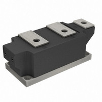
Manufacturer Part Number
VSKT500-12
Description
SCR DBL 2SCR 1200V 500A MAGNAPAK
Manufacturer
Vishay
Datasheet
1.VSKH500-12.pdf
(8 pages)
Specifications of VSKT500-12
Structure
Series Connection - All SCRs
Number Of Scrs, Diodes
2 SCRs
Voltage - Off State
1200V
Current - Gate Trigger (igt) (max)
200mA
Current - On State (it (av)) (max)
500A
Current - On State (it (rms)) (max)
785A
Current - Non Rep. Surge 50, 60hz (itsm)
17800A, 18700A
Current - Hold (ih) (max)
500mA
Mounting Type
Chassis Mount
Package / Case
SUPER MAGN-A-PAK
Rated Repetitive Off-state Voltage Vdrm
1200 V
Off-state Leakage Current @ Vdrm Idrm
100 mA
Holding Current (ih Max)
500 mA
Mounting Style
Screw
Breakover Current Ibo Max
18700 A
Gate Trigger Current (igt)
200 mA
Gate Trigger Voltage (vgt)
3 V
Repetitive Peak Forward Blocking Voltage
1200 V
Lead Free Status / RoHS Status
Contains lead / RoHS non-compliant
Other names
*IRKT500-12
IRKT500-12
IRKT500-12
IRKT500-12
IRKT500-12


VSKT500-..PbF, VSKH500-..PbF, VSKL500-..PbF
Vishay Semiconductors
www.vishay.com
2
ON-STATE CONDUCTION
PARAMETER
Maximum average on-state current
at case temperature
Maximum RMS on-state current
Maximum peak, one-cycle,
non-repetitive on-state surge current
Maximum I
Maximum I
Low level value or threshold voltage
High level value of threshold voltage
Low level value on-state slope resistance
High level value on-state slope resistance
Maximum on-state voltage drop
Maximum forward voltage drop
Maximum holding current
Maximum latching current
SWITCHING
PARAMETER
Maximum rate of rise of turned-on current
Typical delay time
Typical turn-off time
BLOCKING
PARAMETER
Maximum critical rate of rise
of off-state voltage
RMS insulation voltage
Maximum peak reverse and
off-state leakage current
2
2
t for fusing
t for fusing
DiodesAmericas@vishay.com, DiodesAsia@vishay.com,
For technical questions within your region, please contact one of the following:
(SUPER MAGN-A-PAK Power Modules), 500 A
SYMBOL
SYMBOL
SYMBOL
V
V
I
dV/dt
Thyristor/Diode and Thyristor/Thyristor
I
T(RMS)
dI/dt
I
I
I
I
V
I
RRM
T(AV),
T(TO)1
T(TO)2
V
V
F(AV)
TSM,
I
DRM
FSM
2
I
r
r
I
t
t
INS
I
2
TM
FM
t1
t2
H
t
L
d
q
t
,
T
t = 1 s
T
180° conduction, half sine wave
180° conduction, half sine wave at T
t = 10 ms
t = 8.3 ms
t = 10 ms
t = 8.3 ms
t = 10 ms
t = 8.3 ms
t = 10 ms
t = 8.3 ms
t = 0.1 ms to 10 ms, no voltage reapplied
(16.7 % x x I
(I > x I
(16.7 % x x I
(I > x I
I
I
T
T
Gate current 1 A, dI
V
I
V
pk
pk
TM
J
J
J
J
d
R
= 130 °C, linear to V
= T
= 25 °C, anode supply 12 V resistive load
= T
= 0.67 % V
= 1500 A, T
= 1500 A, T
= 50 V, dV/dt = 20 V/μs, gate 0 V 100
= 750 A; T
J
J
maximum, I
maximum, rated V
T(AV)
T(AV)
), T
), T
J
DRM
T(AV)
T(AV)
J
J
J
J
= T
= 25 °C, t
= 25 °C, t
= T
= T
No voltage
reapplied
100 % V
reapplied
No voltage
reapplied
100 % V
reapplied
, T
TEST CONDITIONS
TEST CONDITIONS
TEST CONDITIONS
J
< I < x I
< I < x I
TM
g
J
J
maximum, dI/dt = - 60 A/μs,
J
/dt = 1 A/μs
maximum
maximum
= 25 °C
= 400 A, V
D
= 80 % V
p
p
DRM
RRM
RRM
DiodesEurope@vishay.com
= 10 ms sine pulse
= 10 ms sine pulse
T(AV)
T(AV)
/V
RRM
), T
), T
DRM
DRM
Sinusoidal
half wave,
initial T
J
J
applied
C
= T
= T
applied
= 82 °C
J
J
J
maximum
maximum
= T
J
maximum
Document Number: 94420
VALUES
VALUES
VALUES
15 910
1000
1000
3000
1591
1452
1125
1027
1000
17.8
18.7
15.0
15.7
0.85
0.93
0.36
0.32
1.50
1.50
200
100
500
785
500
2.0
Revision: 02-Jul-10
82
UNITS
UNITS
UNITS
kA
kA
A/μs
V/μs
m
mA
mA
kA
°C
μs
V
A
A
V
V
V
2
2
s
s
Related parts for VSKT500-12
Image
Part Number
Description
Manufacturer
Datasheet
Request
R

Part Number:
Description:
SCR DBL 2SCR 800V 500A MAGNAPAK
Manufacturer:
Vishay
Datasheet:
Part Number:
Description:
SCR DBL 2SCR 1400V 500A MAGNAPAK
Manufacturer:
Vishay
Datasheet:
Part Number:
Description:
SCR DBL 2SCR 1600V 500A MAGNAPAK
Manufacturer:
Vishay
Datasheet:

Part Number:
Description:
SCR Modules 500 Amp 1200 Volt 785 Amp IT(RMS)
Manufacturer:
Vishay
Part Number:
Description:
SCR Modules 500 Amp 1400 Volt 785 Amp IT(RMS)
Manufacturer:
Vishay
Part Number:
Description:
SCR Modules 500 Amp 800 Volt 785 Amp IT(RMS)
Manufacturer:
Vishay
Part Number:
Description:
SCR Modules 500 Amp 1600 Volt 785 Amp IT(RMS)
Manufacturer:
Vishay

Part Number:
Description:
Thyristor/Diode and Thyristor/Thyristor
Manufacturer:
Vishay Siliconix
Datasheet:
Part Number:
Description:
357-036-542-201 CARDEDGE 36POS DL .156 BLK LOPRO
Manufacturer:
Vishay
Datasheet:
Part Number:
Description:
357-036-542-201 CARDEDGE 36POS DL .156 BLK LOPRO
Manufacturer:
Vishay
Datasheet:
Part Number:
Description:
357-036-542-201 CARDEDGE 36POS DL .156 BLK LOPRO
Manufacturer:
Vishay
Datasheet:
Part Number:
Description:
357-036-542-201 CARDEDGE 36POS DL .156 BLK LOPRO
Manufacturer:
Vishay
Datasheet:
Part Number:
Description:
357-036-542-201 CARDEDGE 36POS DL .156 BLK LOPRO
Manufacturer:
Vishay
Datasheet:
Part Number:
Description:
357-036-542-201 CARDEDGE 36POS DL .156 BLK LOPRO
Manufacturer:
Vishay
Datasheet:
Part Number:
Description:
357-036-542-201 CARDEDGE 36POS DL .156 BLK LOPRO
Manufacturer:
Vishay
Datasheet: