STGIPS14K60 STMicroelectronics, STGIPS14K60 Datasheet
STGIPS14K60
Specifications of STGIPS14K60
Available stocks


Related parts for STGIPS14K60


STGIPS14K60 Summary of contents
Page 1
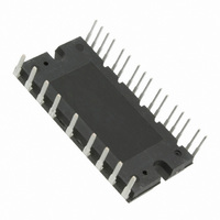
... ICs with the most advanced short-circuit- rugged IGBT system technology, this device is ideal for 3-phase inverters in applications such as home appliances and air conditioners. SLLIMM™ trademark of STMicroelectronics. Marking Package GIPS14K60 SDIP-25L Doc ID 15927 Rev 5 STGIPS14K60 SLLIMM™ SDIP-25L Packaging Tube 1/20 www.st.com 20 ...
Page 2
... Internal block diagram and pin configuration . . . . . . . . . . . . . . . . . . . . 3 2 Electrical ratings . . . . . . . . . . . . . . . . . . . . . . . . . . . . . . . . . . . . . . . . . . . . 5 2.1 Absolute maximum ratings . . . . . . . . . . . . . . . . . . . . . . . . . . . . . . . . . . . . . 5 2.2 Thermal data . . . . . . . . . . . . . . . . . . . . . . . . . . . . . . . . . . . . . . . . . . . . . . . 6 3 Electrical characteristics . . . . . . . . . . . . . . . . . . . . . . . . . . . . . . . . . . . . . 7 3.1 Control part . . . . . . . . . . . . . . . . . . . . . . . . . . . . . . . . . . . . . . . . . . . . . . . . 9 3.2 Waveforms definitions . . . . . . . . . . . . . . . . . . . . . . . . . . . . . . . . . . . . . . . 12 4 Smart shutdown function . . . . . . . . . . . . . . . . . . . . . . . . . . . . . . . . . . . . 13 5 Applications information . . . . . . . . . . . . . . . . . . . . . . . . . . . . . . . . . . . . 14 5.1 Recommendations . . . . . . . . . . . . . . . . . . . . . . . . . . . . . . . . . . . . . . . . . . 15 6 Package mechanical data . . . . . . . . . . . . . . . . . . . . . . . . . . . . . . . . . . . . 16 7 Revision history . . . . . . . . . . . . . . . . . . . . . . . . . . . . . . . . . . . . . . . . . . . 19 2/20 Doc ID 15927 Rev 5 STGIPS14K60 ...
Page 3
... STGIPS14K60 1 Internal block diagram and pin configuration Figure 1. Internal block diagram Pin 1 OUT U VBOOT U LIN-U HIN-U VCC OUT V VBOOT V GND LIN-V HIN-V OUT W VBOOT W LIN-W HIN-W SD/OD CIN Pin 16 Internal block diagram and pin configuration LIN Vboot SD/OD HVG HIN OUT ...
Page 4
... Shut down logic input (active low) / open drain (comparator output) CIN Comparator input N Negative DC input for W phase phase output P Positive DC input N Negative DC input for V phase phase output P Positive DC input N Negative DC input for U phase phase output P Positive DC input Doc ID 15927 Rev 5 STGIPS14K60 Description ...
Page 5
... STGIPS14K60 2 Electrical ratings 2.1 Absolute maximum ratings Table 3. Inverter part Symbol V Supply voltage applied between Supply voltage (surge) applied between PN(surge Each IGBT collector emitter voltage (V CES Each IGBT continuous collector current (2) ± (3) ± I Each IGBT pulsed collector current CP P Each IGBT total dissipation at T ...
Page 6
... Thermal data Table 6. Thermal data Symbol Thermal resistance junction-case single IGBT R thJC Thermal resistance junction-case single diode 6/20 Parameter ≤ 100°C). C Parameter Doc ID 15927 Rev 5 STGIPS14K60 Value Unit 2500 V -40 to 150 °C -40 to 125 °C Value Unit 3 °C/W 5.5 °C/W ...
Page 7
... STGIPS14K60 3 Electrical characteristics °C unless otherwise specified. J Table 7. Inverter part Symbol Parameter Collector-emitter V CE(sat) saturation voltage Collector-cut off current I (1) CES ( “logic state” Diode forward voltage F Inductive load switching time and energy t Turn-on time on t Crossover time (on) c(on) t Turn-off time ...
Page 8
... Note: Figure 4 "Switching time definition" refers to HIN inputs (active high). For LIN inputs (active low), VIN polarity must be inverted for turn-on and turn-off. 8/20 100% I 100 C(ON) 10% I 90 (a) turn-on Doc ID 15927 Rev 5 STGIPS14K60 OFF t C(OFF) 10 IN(OFF) (b) turn-off C AM09223V1 ...
Page 9
... STGIPS14K60 3.1 Control part Table 8. Low voltage power supply (V Symbol Parameter hysteresis cc_hys turn ON threshold cc_thON turn OFF threshold cc_thOFF cc Undervoltage quiescent I qccu supply current I Quiescent current qcc Internal comparator (CIN) V ref reference voltage Table 9. Bootstrapped voltage (V Symbol Parameter hysteresis BS_hys ...
Page 10
... V CP SD/OD pulled through 100 kΩ resistor C = 180 pF kΩ OUT boot 3 Measured applying a voltage step from 3 pin CIN i Logic input ( LIN Doc ID 15927 Rev 5 STGIPS14K60 Min. Typ. Max 0 130 - 125 200 50 200 250 Output HIN LVG Unit 3 µ V/µsec ns HVG ...
Page 11
... STGIPS14K60 Figure 5. Maximum I C(RMS) switching frequency 1. Simulated curves refer to typical IGBT parameters and maximum R current vs. Figure 6. (1) thj-c. Doc ID 15927 Rev 5 Electrical characteristics Maximum I current vs. f C(RMS) (1) SINE 11/20 ...
Page 12
... DT LH HVG gate driver outputs OFF (HALF-BRIDGE TRI-STATE) LIN HIN LVG DT LH HVG gate driver outputs OFF (HALF-BRIDGE TRI-STATE) Doc ID 15927 Rev 5 STGIPS14K60 DT HL gate driver outputs OFF DT HL gate driver outputs OFF (HALF-BRIDGE TRI-STATE gate driver outputs OFF (HALF-BRIDGE TRI-STATE ...
Page 13
... STGIPS14K60 4 Smart shutdown function The STGIPS14K60 integrates a comparator for fault sensing purposes. The comparator non-inverting input (CIN) can be connected to an external shunt resistor in order to implement a simple over-current protection function. When the comparator triggers, the device is set in shutdown state and both its outputs are set to low level leading the half- bridge in tri-state ...
Page 14
... Applications information 5 Applications information Figure 9. Typical application circuit 14/20 CONTROLLER Doc ID 15927 Rev 5 STGIPS14K60 AM05001v1 ...
Page 15
... STGIPS14K60 5.1 Recommendations ● Input signal HIN is active high logic input external RC filter is used, for noise immunity, pay attention to the variation of the input signal level. ● Input signal /LIN is active low logic. A 720 kΩ (typ.) pull-up resistor, connected to an internal 5V regulator through a diode, is built-in for each low side input. ...
Page 16
... Doc ID 15927 Rev 5 STGIPS14K60 ® Max. 44.8 1.75 2 39.8 22.4 12.25 25.63 5.8 7.4 12.1 2.75 4 5.1 6.9 1.2 0.7 2.15 0.7 ...
Page 17
... STGIPS14K60 Figure 10. SDIP-25L drawing dimensions Doc ID 15927 Rev 5 Package mechanical data 8154676 revF 17/20 ...
Page 18
... Package mechanical data Figure 11. SDIP-25L tube dimensions 18/20 Doc ID 15927 Rev 5 STGIPS14K60 8304142_A ...
Page 19
... STGIPS14K60 7 Revision history Table 15. Document revision history Date 25-Jun-2009 05-Aug-2009 15-Jun-2010 08-Nov-2010 09-Mar-2011 Revision 1 Initial release. 2 Reduced V value on CE(sat) Document status promoted from preliminary data to datasheet. Updated package mechanical data, 3 Figure 5: Maximum IC(RMS) current vs. switching frequency and Figure 6: Maximum IC(RMS) current vs. fSINE (1). ...
Page 20
... Australia - Belgium - Brazil - Canada - China - Czech Republic - Finland - France - Germany - Hong Kong - India - Israel - Italy - Japan - Malaysia - Malta - Morocco - Philippines - Singapore - Spain - Sweden - Switzerland - United Kingdom - United States of America 20/20 Please Read Carefully: © 2011 STMicroelectronics - All rights reserved STMicroelectronics group of companies www.st.com Doc ID 15927 Rev 5 STGIPS14K60 ...