CM150DX-24A Powerex Inc, CM150DX-24A Datasheet - Page 3
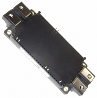
CM150DX-24A
Manufacturer Part Number
CM150DX-24A
Description
IGBT MOD DUAL 1200V 150A NX SER
Manufacturer
Powerex Inc
Series
IGBTMOD™r
Datasheet
1.CM150DX-24A.pdf
(5 pages)
Specifications of CM150DX-24A
Configuration
Half Bridge
Voltage - Collector Emitter Breakdown (max)
1200V
Vce(on) (max) @ Vge, Ic
2.6V @ 15V, 150A
Current - Collector (ic) (max)
150A
Current - Collector Cutoff (max)
1mA
Input Capacitance (cies) @ Vce
23nF @ 10V
Power - Max
960W
Input
Standard
Ntc Thermistor
Yes
Mounting Type
Chassis Mount
Package / Case
Module
Dc Collector Current
150A
Collector Emitter Voltage Vces
1.2kV
Power Dissipation Pd
10mW
Collector Emitter Voltage V(br)ceo
1.2kV
Operating Temperature Range
-40°C To +150°C
No. Of Pins
11
Lead Free Status / RoHS Status
Lead free / RoHS Compliant
For Use With
BG2B-5015 - KIT DEV BOARD 2CN 5A FOR IGBTBG2B-3015 - KIT DEV BOARD 2CN 3A FOR IGBTBG2B-1515 - KIT DEV BOARD 1.5A FOR IGBTBG2A-NF - KIT DEV BOARD FOR IGBT
Igbt Type
-
Lead Free Status / RoHS Status
Lead free / RoHS Compliant, Lead free / RoHS Compliant
Other names
835-1008


Powerex, Inc., 173 Pavilion Lane, Youngwood, Pennsylvania 15697 (724) 925-7272
CM150DX-24A
Dual IGBTMOD™ NX-Series Module
150 Amperes/1200 Volts
Rev. 3/09
Electrical and Mechanical Characteristics, T
Inverter Sector
Characteristics
Collector Cutoff Current
Gate-Emitter Threshold Voltage
Gate Leakage Current
Collector-Emitter Saturation Voltage
Input Capacitance
Output Capacitance
Reverse Transfer Capacitance
Total Gate Charge
Inductive
Load
Switch
Time
Reverse Recovery Time
Reverse Recovery Charge
Emitter-Collector Voltage
Thermal and Mechanical Characteristics, T
Characteristics
Module Lead Resistance
Thermal Resistance, Junction to Case**
Thermal Resistance, Junction to Case**
Contact Thermal Resistance**
Internal Gate Resistance
External Gate Resistance
NTC Thermistor Sector, T
Characteristics
Zero Power Resistance
Deviation of Resistance
B Constant
Power Dissipation
**Thermal resistance values are per 1 element.
*1 Case temperature (T
*2 I
*5 Pulse width and repetition rate should be such as to cause negligible temperature rise.
*6 R
*7 Typical value is measured by using thermally conductive grease of λ = 0.9 [W/(m • K)].
E
1
, I
: Resistance at Absolute Temperature T
EM
, V
EC
, t
rr
and Q
C
) and heatsink temperature (T
rr
Turn-on Delay Time
Turn-on Rise Time
Turn-off Delay Time
Turn-off Fall Time
represent ratings and characteristics of the anti-parallel, emitter-to-collector free-wheel diode (FWDi).
j
= 25°C unless otherwise specified
1
(K), R
R
R
V
2
B
V
Symbol
Symbol
R
Symbol
: Resistance at Absolute Temperature T
V
CE(sat)
t
t
R
th(j-c)
R
∆R/R
f
th(j-c)
(25/50)
I
I
C
Qrr
GE(th)
C
C
R
) are defined on the surface of the baseplate and heatsink at just under the chip.
d(on)
d(off)
CES
GES
t
th(c-f)
P
Q
R
EC
rr
lead
Gint
oes
res
t
t
TH
ies
25
r
G
f
G
*2
*2
*2
Q
D
j
j
= 25°C unless otherwise specified
= 25°C unless otherwise specified
Inductive Load Switching Operation
V
B = (InR
Main Termnals-Chip (Per Switch)
Case to Heatsink (Per 1 Module)
CC
I
C
I
I
I
E
C
Thermal Grease Applied
T
E
= 150A, V
= 600V, I
C
= 150A, V
= 150A, V
V
I
= 150A, V
C
R
I
V
CC
E
= 100°C, R
V
V
G
I
CE
= 150A, V
1
C
= 150A, V
CE
GE
= 2.2Ω, I
Test Conditions
Test Conditions
= 600V, I
– InR
= 15mA, V
V
T
T
= 10V, V
Test Conditions
Per FWDi
Per IGBT
T
GE
= V
= V
C
C
C
C
GE
GE
= 25°C
= 25°C
GE
GE
= 150A, V
= 25°C
CES
GES
= ±15V,
2
) / (1/T
= 15V, T
GE
100
= 0V, T
GE
= 15V, T
E
= 0V, T
C
GE
, V
, V
2
= 150A,
CE
*1
(K), T(K) = T(°C) + 273.15
= 150A,
*1
= 15V, Chip
*1
*1
= 0V, Chip
= 493Ω
GE
CE
= 0V
1
= 10V
GE
j
– 1/T
j
j
= 0V
= 0V
= 125°C
j
= 125°C
= 25°C
= 25°C
*1*7
= 15V
*1
2
)
*6
*5
*5
*5
*5
4.85
Min.
Min.
Min.
–7.3
—
—
—
—
—
—
—
—
—
—
—
—
—
—
—
—
—
—
—
—
—
—
—
—
—
6
2
0.015
3375
2.16
5.00
675
Typ.
Typ.
Typ.
2.0
2.2
2.6
2.5
1.9
1.6
—
—
—
—
—
—
—
—
—
—
—
—
—
—
—
7
6
0
Max.
Max.
Max.
23.0
0.45
0.13
0.23
5.15
+7.8
130
100
450
600
150
0.5
2.6
2.0
3.4
1.0
21
—
—
—
—
—
—
—
—
—
—
10
8
°C/W
°C/W
°C/W
Units
Volts
Volts
Volts
Volts
Volts
Volts
Volts
Units
Units
mW
mΩ
mA
nC
µC
kΩ
µA
nF
nF
nF
ns
ns
ns
ns
ns
%
Ω
Ω
K
3
Related parts for CM150DX-24A
Image
Part Number
Description
Manufacturer
Datasheet
Request
R

Part Number:
Description:
Manufacturer:
Powerex Inc
Datasheet:

Part Number:
Description:
SWITCH REED 15-25AT SPST SMD
Manufacturer:
Coto Technology
Datasheet:
Part Number:
Description:
SWITCH REED 15-20AT SPST SMD
Manufacturer:
Coto Technology
Datasheet:
Part Number:
Description:
SWITCH REED 10-30AT SPST SMD
Manufacturer:
Coto Technology
Datasheet:
Part Number:
Description:
SWITCH REED 20-25AT SPST SMD
Manufacturer:
Coto Technology
Datasheet:
Part Number:
Description:
SWITCH REED 10-20AT SPST SMD
Manufacturer:
Coto Technology
Datasheet:
Part Number:
Description:
SWITCH REED 10-15AT SPST SMD
Manufacturer:
Coto Technology
Datasheet:


Part Number:
Description:
Switch Fabric, Tip-Over Switches
Manufacturer:
Comus Group of Companies
Part Number:
Description:
Manufacturer:
Powerex Inc
Datasheet:
Part Number:
Description:
Manufacturer:
Powerex Inc
Datasheet:
Part Number:
Description:
Manufacturer:
Powerex Inc
Datasheet:
Part Number:
Description:
Manufacturer:
Powerex Inc
Datasheet:
Part Number:
Description:
Manufacturer:
Powerex Inc
Datasheet: