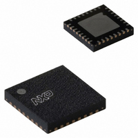
PN5110A0HN1/C2,118 NXP Semiconductors, PN5110A0HN1/C2,118 Datasheet - Page 4

PN5110A0HN1/C2,118
Manufacturer Part Number
PN5110A0HN1/C2,118
Description
IC TRANSMISSION MOD 32-HVQFN
Manufacturer
NXP Semiconductors
Datasheet
1.PN5110A0HN1C2118.pdf
(22 pages)
Specifications of PN5110A0HN1/C2,118
Rf Type
Read / Write
Frequency
13.56MHz
Features
ISO14443A / Mifare
Package / Case
32-VQFN Exposed Pad, 32-HVQFN, 32-SQFN, 32-DHVQFN
Lead Free Status / RoHS Status
Lead free / RoHS Compliant
Other names
935280541118
PN5110A0HN1/C2-T
PN5110A0HN1/C2-T
PN5110A0HN1/C2-T
PN5110A0HN1/C2-T
NXP Semiconductors
4. Quick reference data
Table 1.
[1]
[2]
[3]
[4]
[5]
[6]
[7]
[8]
5. Ordering information
Table 2.
082733
Product short data sheet
Symbol
AV
DV
TV
PV
I
I
I
I
I
I
I
T
Type number
PN5110A0HN1/C2
PN5110A0HN/C2
HPD
SPD
DVDD
AVDD
AVDD,RCVOFF
PVDD
TVDD
amb
DD
DD
DD
DD
Supply voltage below 3 V reduces the performance (e.g. the achievable operating distance).
AV
PV
I
I
During operation with a typical circuitry the overall current is below 100 mA.
I
Typical value using a complementary driver configuration and an antenna matched to 40 Ω between TX1 and TX2 at 13.56 MHz
TVDD
PVDD
SPD
DD
DD
and I
, DV
depends on TV
depends on the overall load at the digital pins.
shall always be on the same or lower voltage level than DV
Quick reference data
Ordering information
DD
HPD
Parameter
Supply Voltage
Hard Power-down Current
Soft Power-down Current
Digital Supply Current
Analog Supply Current
Analog Supply Current,
receiver switched off
Pad Supply Current
Transmitter Supply Current
operating ambient temperature
and TV
are the total currents over all supplies.
Package
Name
HVQFN32
HVQFN40
DD
DD
shall always be on the same voltage level.
and the external circuitry connected to Tx1 and Tx2
Description
Plastic thermal enhanced very thin quad flat package; no leads;
32 terminals; body 5 × 5 × 0.85 mm
Plastic thermal enhanced very thin quad flat package; no leads;
40 terminals; body 6× 6× 0.85 mm
Conditions
AV
PV
AV
TV
N
AV
3 V, RF level detector on
AV
AV
Continuous Wave
DV
RESET
Rev. 3.3 — 13 June 2007
SS
DD
DD
DD
DD
DD
DD
DD
= DV
= DV
= 3 V, bit RCVOff = 0
= PV
= DV
= 3 V, bit RCVOff = 1
≤ AV
= 3 V
= LOW
SS
DD
DD
DD
DD
= PV
= 3 V,
DD
= DV
=
= TV
.
SS
DD
DD
= TV
= PV
=TV
SS
DD
DD
= 0 V,
=
[1][2]
[1][2]
[1][2]
[3]
[7]
[7]
[5]
[4][6][8]
Min
2.5
1.6
-
-
-
-
-
-
-
-30
Transmission Module
Typ
-
-
-
-
6.5
7
3
-
60
© NXP B.V. 2007. All rights reserved.
Max
3.6
3.6
5
10
9
10
5
40
100
+85
PN511
Version
SOT617
SOT618
Unit
V
V
μA
μA
mA
mA
mA
mA
mA
°C
4 of 22


