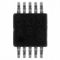
TDK5110F Infineon Technologies, TDK5110F Datasheet - Page 32

TDK5110F
Manufacturer Part Number
TDK5110F
Description
TRANSMITTER ASK/FSK SGL TSSOP10
Manufacturer
Infineon Technologies
Type
Transmitterr
Specifications of TDK5110F
Package / Case
10-TSSOP
Frequency
434MHz Center
Applications
Alarm Systems, Communication Systems
Modulation Or Protocol
ASK, FSK
Data Rate - Maximum
20 kbps
Power - Output
11dBm
Current - Transmitting
14.2mA
Data Interface
PCB, Surface Mount
Antenna Connector
PCB, Surface Mount
Voltage - Supply
2.1 V ~ 4 V
Operating Temperature
-40°C ~ 125°C
Operating Frequency
870 MHz
Operating Supply Voltage
2.5 V, 3.3 V
Maximum Operating Temperature
+ 125 C
Minimum Operating Temperature
- 40 C
Mounting Style
SMD/SMT
Lead Free Status / RoHS Status
Lead free / RoHS Compliant
Features
-
Memory Size
-
Lead Free Status / RoHS Status
Lead free / RoHS Compliant, Lead free / RoHS Compliant
Other names
SP000056180
TDK5110FXT
TDK5110FXT
Available stocks
Company
Part Number
Manufacturer
Quantity
Price
Company:
Part Number:
TDK5110F
Manufacturer:
INF
Quantity:
9 999
Company:
Part Number:
TDK5110F
Manufacturer:
INFINEON
Quantity:
616
Part Number:
TDK5110F
Manufacturer:
INFINEON/英飞凌
Quantity:
20 000
Please note that f
Table 10
1) a) When the minimum T
All three measures can be taken independently and additive.
2) Derating linearly to a saturation voltage of max. 140 mV at I
3) Matching circuitry as used in the 50 Ohm-Output Testboard.
Data Sheet
Parameter
Power Amplifier Output (Pin 9)
Output Power
434 MHz
transformed to
50 Ohm.
Power Down Mode Control (Pin 10)
Power Down mode
PLL Enable mode
Transmit mode
Input bias current
PDWN
b) When the maximum T
c) When the minimum V
Restriction of c): The maximum f
Tolerances of the passive elements not taken into account.
Range @ 2.1 V, +25°C: 6.5 dBm +/- 2 dBm
Range @ 3.0 V, +25°C: 10 dBm +/- 3 dBm
Range @ 4.0 V, +25°C: 11.5 dBm +4.5/-3.5 dBm
VCO
Supply Voltage V
3)
is twice the Output Frequency.
at
A
S
A
is increased by 5°C, the minimum f
is increased by 25 mV, the maximum f
is decreased by 5°C, the maximum f
Symbol
P
P
P
V
V
V
I
PDWN
OUT, 434
OUT, 434
OUT, 434
PDWN
PDWN
PDWN
VCO
must not be increased by more than 40 MHz by increasing V
S
=2.1V ... 4.0V, T
min.
4
6
6.5
0
1.5
1.5
Limit Values
32
typ.
6.5
10
11.5
CLKOUT
VCO
amb
VCO
VCO
decreases by 1 MHz.
=-40°C ... +125°C (cont’d)
16
= 0 mA
max.
9.5
13
0.5
V
V
38
increases by 1 MHz.
increases by 1 MHz.
S
S
Unit Test
dBm V
dBm V
dBm V
V
V
V
µA
Conditions
V
V
V
V
V
V 1.1, 2006-07-10
S
S
S
ASKDTA
FSKDTA
ASKDTA
ASKDTA
PDWN
= 2.1 V
= 3.0 V
= 4.0 V
TDK5110F
Reference
= V
S
< 0.2 V
< 0.2 V
< 0.5 V
> 1.5 V
.
S


