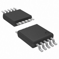
ATA5749-6DPY Atmel, ATA5749-6DPY Datasheet - Page 20

ATA5749-6DPY
Manufacturer Part Number
ATA5749-6DPY
Description
IC XMITTER FRACT-N PLL 10TSSOP
Manufacturer
Atmel
Datasheet
1.ATA5749-6DQY.pdf
(26 pages)
Specifications of ATA5749-6DPY
Frequency
300MHz ~ 450MHz
Applications
General Data Transfer
Modulation Or Protocol
ASK, FSK
Data Rate - Maximum
40 kbps
Power - Output
12.5dBm
Current - Transmitting
8.8mA
Data Interface
PCB, Surface Mount
Antenna Connector
PCB, Surface Mount
Voltage - Supply
1.9 V ~ 3.6 V
Operating Temperature
-40°C ~ 125°C
Package / Case
10-TSSOP
Lead Free Status / RoHS Status
Lead free / RoHS Compliant
Features
-
Memory Size
-
10. Electrical Characteristics (Continued)
V
f
C
20
*) Type means: A = 100% tested, B = 100% correlation tested, C = Characterized on samples, D = Design parameter
Note:
CLK
3.10
3.11
S
0
No. Parameters
3.5
3.6
3.7
3.8
3.9
4.1
4.2
4.3
4.4
4.5
4
= 1.9V to 3.6V T
= 1.5pF, C
= 1.625MHz unless otherwise specified. If crystal parameters are important values correspond to a crystal with C
Locking time of the PLL
DC voltage after XTAL
amplitude stable
Negative real part of
XTO impedance at
begin of start-up
External Capacitors
C4, C5
Pin Capacitance
XTO1 and XTO2
Crystal oscillator
start-up time
Maximum shunt
capacitance C
Oscillator frequency
XTO
Fractional-N-PLL
Frequency range of RF
frequency
PLL loop bandwidth
In Loop phase noise
PLL
Out of Loop Phase
noise (VCO)
(Pin Number) in brackets mean they are measured matched to 50 according to
and optimum load impedances according to
Atmel ATA5749
LOAD
= 9pF and R
amb
0
= –40°C to +125°C, CLK_ON = “High”; DIV_CNTRL = “Low”, CLOAD_CLK = 10pF. f
of XTAL
M
Test Conditions
V(XTO2) – V(XTO1)
XTO running
This value is important for
crystal oscillator start-up
behavior
C
8pF < C
F
11.0MHz < F
Recommended values for proper
start-up and low current
consumption
Quality NPO
C
(C
(C
C
The PCB Capacitance of about
1pF has to be added
Time between EN = “High” and
XTO_RDY = “High”
C
C
R
11.0MHz < F
Required for stable operation of
XTO, C
433.92MHz and 315MHz other
frequencies
S434_N315 = “LOW”
S434_N315 = “HIGH”
Time between
XTO_RDY= “High” and Register
programmed till PLL is locked
f
other f
Unity gain loop frequency of
synthesizer
25kHz distance to carrier
At 1MHz
At 36MHz
XTO
XTAL
0
LOAD
Load_nom
0
0
M
170 . Typical values are given at V
5
4
< 2.0pF, 4fF < C
< 2.0pF, 2fF < C
< 2.0pF,
< 170
+ C
+ C
= 13.0000MHz
= 13.000MHz
= (C
XTO
Load
XTO2
5
LOAD
+ C
= 9pF (inc. PCB)
4
> 7. 5pF
) /
+ C
XTO1
< 10pF
XTAL
XTAL
XTO1
+ C
< 14.8MHz
< 14.8MHz
M
M
)
XTO2
< 15fF
< 15fF
Table 4-1
)
and
6, 7, 1
6, 7
6, 7
6, 7
6, 7
6, 7
6, 7
1, 5
Pin
Table 4-2 on page 9
5
5
5
5
S
= 3.0V and T
R
XTO12_START
Symbol
V
f
C
Loop_PLL
C
C
L
DC_XTO
L
L
f
0_MAX
T
at36M
T
XTO
f
C
C
XTO1
XTO2
at1M
RF
PLL
XTO
PLL
4
5
amb
= 25°C
–1,500
–1,300
–15%
–15%
Min.
–5%
11.0
Figure 4-2 on page 8
300
367
140
13.0000
–2,200
–122
Typ.
0.20
0.32
280
–83
–91
1.5
40
15
2
2
XTO
+15%
+15%
1280/
98.46
Max.
–115
+5%
f
14.8
368
450
380
–76
–84
0.3
0.5
3.0
XTO
= 13.0000MHz,
with component values
M
dBc/Hz
dBc/Hz
dBc/Hz
= 4.0fF,
MHz
MHz
Unit
kHz
mV
ms
pF
pF
pF
µs
9128G–RKE–03/11
Type*
C
B
D
C
B
D
C
A
B
B
A
A
C


