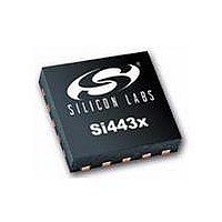
SI4430-B1-FM Silicon Laboratories Inc, SI4430-B1-FM Datasheet - Page 50

SI4430-B1-FM
Manufacturer Part Number
SI4430-B1-FM
Description
IC TXRX 900-960MHZ -8-13DB 20QFN
Manufacturer
Silicon Laboratories Inc
Specifications of SI4430-B1-FM
Package / Case
20-VQFN
Mfg Application Notes
Transitioning SI4430/31 to Rev B
Frequency
900MHz ~ 960MHz
Data Rate - Maximum
256kbps
Modulation Or Protocol
ISM
Applications
General Purpose
Power - Output
13dBm
Sensitivity
-121dBm
Voltage - Supply
1.8 V ~ 3.6 V
Current - Receiving
18.5mA
Current - Transmitting
30mA
Data Interface
PCB, Surface Mount
Antenna Connector
PCB, Surface Mount
Operating Temperature
-40°C ~ 85°C
Wireless Frequency
900 MHz to 960 MHz
Output Power
13 dBm
Operating Supply Voltage
1.8 V to 3.6 V
Maximum Operating Temperature
+ 85 C
Mounting Style
SMD/SMT
Maximum Supply Current
30 mA
Minimum Operating Temperature
- 40 C
Modulation
FSK, GFSK, OOK
Lead Free Status / RoHS Status
Lead free / RoHS Compliant
Memory Size
-
Lead Free Status / Rohs Status
Lead free / RoHS Compliant
Available stocks
Company
Part Number
Manufacturer
Quantity
Price
Company:
Part Number:
SI4430-B1-FM
Manufacturer:
Silicon Labs
Quantity:
135
Part Number:
SI4430-B1-FM
Manufacturer:
SILICON LABS/芯科
Quantity:
20 000
Si4430/31/32-B1
8. Auxiliary Functions
8.1. Smart Reset
The Si4430/31/32 contains an enhanced integrated SMART RESET or POR circuit. The POR circuit contains both
a classic level threshold reset as well as a slope detector POR. This reset circuit was designed to produce a
reliable reset signal under any circumstances. Reset will be initiated if any of the following conditions occur:
The reset will initialize all registers to their default values. The reset signal is also available for output and use by
the microcontroller by using the default setting for GPIO_0. The inverted reset signal is available by default on
GPIO_1.
50
Initial power on, VDD starts from gnd: reset is active till VDD reaches V
When VDD decreases below V
A software reset via “Register 08h. Operating Mode and Function Control 2”: reset is active for time T
On the rising edge of a VDD glitch when the supply voltage exceeds the following time functioned limit:
Release Reset Voltage
Power-On VDD Slope
Low VDD Limit
Software Reset Pulse
Threshold Voltage
Reference Slope
VDD Glitch Reset Pulse
Parameter
VDD starts to rise
0.4V
LD
Figure 26. POR Glitch Parameters
TSWRST
for any reason: reset is active till VDD reaches V
Symbol
SVDD
VTSD
VRR
VDD(t)
VLD
TP
k
Table 15. POR Parameters
t=0,
VDD nom.
Also occurs after SDN, and
VLD<VRR is guaranteed
tested VDD slope region
Rev 1.1
initial power on
reset:
Vglitch>=0.4+t*0.2V/ms
Comment
showing glitch
actual VDD(t)
Reset
0.4V+t*0.2V/ms
T
P
reset limit:
RR
(see table);
t
0.85
0.03
Min
0.7
50
5
RR
;
Typ
1.3
0.4
0.2
16
1
1.75
Max
300
470
1.3
40
SWRST
V/ms
V/ms
Unit
ms
us
V
V
V


