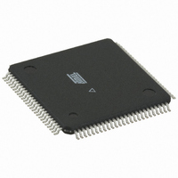
ATMEGA256RZBV-8AU Atmel, ATMEGA256RZBV-8AU Datasheet - Page 15

ATMEGA256RZBV-8AU
Manufacturer Part Number
ATMEGA256RZBV-8AU
Description
MCU ATMEGA2560/AT86RF230 100TQFP
Manufacturer
Atmel
Series
ATMEGAr
Datasheets
1.ATMEGA640V-8CU.pdf
(38 pages)
2.ATMEGA640V-8CU.pdf
(444 pages)
3.AT86RF230-ZU.pdf
(98 pages)
Specifications of ATMEGA256RZBV-8AU
Frequency
2.4GHz
Modulation Or Protocol
802.15.4 Zigbee
Applications
ISM, ZigBee™
Power - Output
3dBm
Sensitivity
-101dBm
Voltage - Supply
1.8 V ~ 3.6 V
Current - Receiving
15.5mA
Current - Transmitting
16.5mA
Data Interface
PCB, Surface Mount
Memory Size
256kB Flash, 4kB EEPROM, 8kB RAM
Antenna Connector
PCB, Surface Mount
Package / Case
100-TQFP
Wireless Frequency
2.4 GHz
Interface Type
JTAG, SPI
Output Power
3 dBm
Operating Temperature Range
- 55 C to + 125 C
For Use With
ATAVRISP2 - PROGRAMMER AVR IN SYSTEMATJTAGICE2 - AVR ON-CHIP D-BUG SYSTEM
Lead Free Status / RoHS Status
Lead free / RoHS Compliant
Operating Temperature
-
Data Rate - Maximum
-
Lead Free Status / Rohs Status
Lead free / RoHS Compliant
For Use With/related Products
ATmega256
Figure 6-11. Packet Structure - SRAM Write Access
Figure 6-12. Packet Structure - SRAM Read Access
Figure 6-13. Example SPI Sequence – SRAM Write Access Sequence of a 5 byte Data Package
SCLK
MOSI
MISO
5131E-MCU Wireless-02/09
SEL
COMMAND
XX
ADDRESS
The SRAM access mode is useful, for instance, if a transmit frame is already stored in
the Frame Buffer and certain bytes (e.g. sequence number or address field) need to be
replaced before retransmitting the frame. Furthermore, it can be used to access only
the LQI value after frame reception. A detailed description of the user accessible frame
content can be found in section 9.3.2.
Each access starts by setting SEL = L. The first transferred byte on MOSI shall be the
command byte and must indicate a SRAM access mode according to the definition in
Table 6-2. The following byte indicates the start address of the write or read access.
The address space is 0x00 to 0x7F. The microcontroller software has to ensure to
access only to the valid address space.
On SRAM write access, one or more bytes of write data are transferred on MOSI
starting with the third byte of the access sequence (see Figure 6-11).
On SRAM read access, one or more bytes of read data are transferred on MISO
starting with the third byte of the access sequence (see Figure 6-12).
As long as SEL is logic low, every subsequent byte read or write increments the
address counter of the Frame Buffer until the SRAM access is terminated by setting
Figure 6-13 and Figure 6-14 illustrate an example SPI sequence of a SRAM access to
write and read a data package of 5 byte length respectively.
XX
SEL = H.
DATA 1
XX
DATA 2
XX
DATA 3
XX
DATA 4
XX
AT86RF230
DATA 5
XX
15


