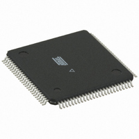
ATMEGA256RZBV-8AU Atmel, ATMEGA256RZBV-8AU Datasheet - Page 37

ATMEGA256RZBV-8AU
Manufacturer Part Number
ATMEGA256RZBV-8AU
Description
MCU ATMEGA2560/AT86RF230 100TQFP
Manufacturer
Atmel
Series
ATMEGAr
Datasheets
1.ATMEGA640V-8CU.pdf
(38 pages)
2.ATMEGA640V-8CU.pdf
(444 pages)
3.AT86RF230-ZU.pdf
(98 pages)
Specifications of ATMEGA256RZBV-8AU
Frequency
2.4GHz
Modulation Or Protocol
802.15.4 Zigbee
Applications
ISM, ZigBee™
Power - Output
3dBm
Sensitivity
-101dBm
Voltage - Supply
1.8 V ~ 3.6 V
Current - Receiving
15.5mA
Current - Transmitting
16.5mA
Data Interface
PCB, Surface Mount
Memory Size
256kB Flash, 4kB EEPROM, 8kB RAM
Antenna Connector
PCB, Surface Mount
Package / Case
100-TQFP
Wireless Frequency
2.4 GHz
Interface Type
JTAG, SPI
Output Power
3 dBm
Operating Temperature Range
- 55 C to + 125 C
For Use With
ATAVRISP2 - PROGRAMMER AVR IN SYSTEMATJTAGICE2 - AVR ON-CHIP D-BUG SYSTEM
Lead Free Status / RoHS Status
Lead free / RoHS Compliant
Operating Temperature
-
Data Rate - Maximum
-
Lead Free Status / Rohs Status
Lead free / RoHS Compliant
For Use With/related Products
ATmega256
- Current page: 37 of 444
- Download datasheet (10Mb)
8.3
8.3.1
8.3.2
8.3.3
8.4
8.4.1
2549M–AVR–09/10
General Purpose registers
External Memory registers
GPIOR2 – General Purpose I/O Register 2
GPIOR1 – General Purpose I/O Register 1
GPIOR0 – General Purpose I/O Register 0
XMCRA – External Memory Control Register A
• Bit 0 – EERE: EEPROM Read Enable
The EEPROM Read Enable Signal EERE is the read strobe to the EEPROM. When the correct
address is set up in the EEAR Register, the EERE bit must be written to a logic one to trigger the
EEPROM read. The EEPROM read access takes one instruction, and the requested data is
available immediately. When the EEPROM is read, the CPU is halted for four cycles before the
next instruction is executed.
The user should poll the EEPE bit before starting the read operation. If a write operation is in
progress, it is neither possible to read the EEPROM, nor to change the EEAR Register.
• Bit 7 – SRE: External SRAM/XMEM Enable
Writing SRE to one enables the External Memory Interface.The pin functions AD7:0, A15:8,
ALE, WR, and RD are activated as the alternate pin functions. The SRE bit overrides any pin
direction settings in the respective data direction registers. Writing SRE to zero, disables the
External Memory Interface and the normal pin and data direction settings are used.
• Bit 6:4 – SRL2:0: Wait-state Sector Limit
It is possible to configure different wait-states for different External Memory addresses. The
external memory address space can be divided in two sectors that have separate wait-state bits.
The SRL2, SRL1, and SRL0 bits select the split of the sectors, see
Bit
0x2B (0x4B)
Read/Write
Initial Value
Bit
0x2A (0x4A)
Read/Write
Initial Value
Bit
0x1E (0x3E)
Read/Write
Initial Value
Bit
“(0x74)”
Read/Write
Initial Value
MSB
MSB
MSB
R/W
R/W
R/W
SRE
R/W
7
0
7
0
7
0
7
0
SRL2
R/W
R/W
R/W
R/W
6
0
6
0
6
0
6
0
ATmega640/1280/1281/2560/2561
SRL1
R/W
R/W
R/W
R/W
5
0
5
0
5
0
5
0
SRL0
R/W
R/W
R/W
R/W
4
0
4
0
4
0
4
0
SRW11
R/W
R/W
R/W
R/W
3
0
3
0
3
0
3
0
SRW10
R/W
R/W
R/W
R/W
2
0
2
0
2
0
2
0
Table 8-2 on page 38
SRW01
R/W
R/W
R/W
R/W
1
0
1
0
1
0
1
0
SRW00
LSB
LSB
LSB
R/W
R/W
R/W
R/W
0
0
0
0
0
0
0
0
GPIOR2
GPIOR1
GPIOR0
XMCRA
and
37
Related parts for ATMEGA256RZBV-8AU
Image
Part Number
Description
Manufacturer
Datasheet
Request
R

Part Number:
Description:
DEV KIT FOR AVR/AVR32
Manufacturer:
Atmel
Datasheet:

Part Number:
Description:
INTERVAL AND WIPE/WASH WIPER CONTROL IC WITH DELAY
Manufacturer:
ATMEL Corporation
Datasheet:

Part Number:
Description:
Low-Voltage Voice-Switched IC for Hands-Free Operation
Manufacturer:
ATMEL Corporation
Datasheet:

Part Number:
Description:
MONOLITHIC INTEGRATED FEATUREPHONE CIRCUIT
Manufacturer:
ATMEL Corporation
Datasheet:

Part Number:
Description:
AM-FM Receiver IC U4255BM-M
Manufacturer:
ATMEL Corporation
Datasheet:

Part Number:
Description:
Monolithic Integrated Feature Phone Circuit
Manufacturer:
ATMEL Corporation
Datasheet:

Part Number:
Description:
Multistandard Video-IF and Quasi Parallel Sound Processing
Manufacturer:
ATMEL Corporation
Datasheet:

Part Number:
Description:
High-performance EE PLD
Manufacturer:
ATMEL Corporation
Datasheet:

Part Number:
Description:
8-bit Flash Microcontroller
Manufacturer:
ATMEL Corporation
Datasheet:

Part Number:
Description:
2-Wire Serial EEPROM
Manufacturer:
ATMEL Corporation
Datasheet:


