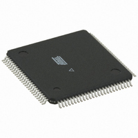
ATMEGA256RZBV-8AU Atmel, ATMEGA256RZBV-8AU Datasheet - Page 241

ATMEGA256RZBV-8AU
Manufacturer Part Number
ATMEGA256RZBV-8AU
Description
MCU ATMEGA2560/AT86RF230 100TQFP
Manufacturer
Atmel
Series
ATMEGAr
Datasheets
1.ATMEGA640V-8CU.pdf
(38 pages)
2.ATMEGA640V-8CU.pdf
(444 pages)
3.AT86RF230-ZU.pdf
(98 pages)
Specifications of ATMEGA256RZBV-8AU
Frequency
2.4GHz
Modulation Or Protocol
802.15.4 Zigbee
Applications
ISM, ZigBee™
Power - Output
3dBm
Sensitivity
-101dBm
Voltage - Supply
1.8 V ~ 3.6 V
Current - Receiving
15.5mA
Current - Transmitting
16.5mA
Data Interface
PCB, Surface Mount
Memory Size
256kB Flash, 4kB EEPROM, 8kB RAM
Antenna Connector
PCB, Surface Mount
Package / Case
100-TQFP
Wireless Frequency
2.4 GHz
Interface Type
JTAG, SPI
Output Power
3 dBm
Operating Temperature Range
- 55 C to + 125 C
For Use With
ATAVRISP2 - PROGRAMMER AVR IN SYSTEMATJTAGICE2 - AVR ON-CHIP D-BUG SYSTEM
Lead Free Status / RoHS Status
Lead free / RoHS Compliant
Operating Temperature
-
Data Rate - Maximum
-
Lead Free Status / Rohs Status
Lead free / RoHS Compliant
For Use With/related Products
ATmega256
- Current page: 241 of 444
- Download datasheet (10Mb)
23. 2-wire Serial Interface
23.1
23.2
23.2.1
2549M–AVR–09/10
Features
2-wire Serial Interface Bus Definition
TWI Terminology
•
•
•
•
•
•
•
•
•
•
The 2-wire Serial Interface (TWI) is ideally suited for typical microcontroller applications. The
TWI protocol allows the systems designer to interconnect up to 128 different devices using only
two bi-directional bus lines, one for clock (SCL) and one for data (SDA). The only external hard-
ware needed to implement the bus is a single pull-up resistor for each of the TWI bus lines. All
devices connected to the bus have individual addresses, and mechanisms for resolving bus
contention are inherent in the TWI protocol.
Figure 23-1. TWI Bus Interconnection
The following definitions are frequently encountered in this section.
Table 23-1.
Term
Master
Slave
Transmitter
Receiver
Simple yet Powerful and Flexible Communication Interface, only two Bus Lines needed
Both Master and Slave Operation Supported
Device can Operate as Transmitter or Receiver
7-bit Address Space Allows up to 128 Different Slave Addresses
Multi-master Arbitration Support
Up to 400 kHz Data Transfer Speed
Slew-rate Limited Output Drivers
Noise Suppression Circuitry Rejects Spikes on Bus Lines
Fully Programmable Slave Address with General Call Support
Address Recognition Causes Wake-up When AVR is in Sleep Mode
SDA
SCL
TWI Terminology
Description
The device that initiates and terminates a transmission. The Master also generates the
SCL clock.
The device addressed by a Master.
The device placing data on the bus.
The device reading data from the bus.
Device 1
Device 2
ATmega640/1280/1281/2560/2561
Device 3
........
Device n
V
CC
R1
R2
241
Related parts for ATMEGA256RZBV-8AU
Image
Part Number
Description
Manufacturer
Datasheet
Request
R

Part Number:
Description:
DEV KIT FOR AVR/AVR32
Manufacturer:
Atmel
Datasheet:

Part Number:
Description:
INTERVAL AND WIPE/WASH WIPER CONTROL IC WITH DELAY
Manufacturer:
ATMEL Corporation
Datasheet:

Part Number:
Description:
Low-Voltage Voice-Switched IC for Hands-Free Operation
Manufacturer:
ATMEL Corporation
Datasheet:

Part Number:
Description:
MONOLITHIC INTEGRATED FEATUREPHONE CIRCUIT
Manufacturer:
ATMEL Corporation
Datasheet:

Part Number:
Description:
AM-FM Receiver IC U4255BM-M
Manufacturer:
ATMEL Corporation
Datasheet:

Part Number:
Description:
Monolithic Integrated Feature Phone Circuit
Manufacturer:
ATMEL Corporation
Datasheet:

Part Number:
Description:
Multistandard Video-IF and Quasi Parallel Sound Processing
Manufacturer:
ATMEL Corporation
Datasheet:

Part Number:
Description:
High-performance EE PLD
Manufacturer:
ATMEL Corporation
Datasheet:

Part Number:
Description:
8-bit Flash Microcontroller
Manufacturer:
ATMEL Corporation
Datasheet:

Part Number:
Description:
2-Wire Serial EEPROM
Manufacturer:
ATMEL Corporation
Datasheet:


