MRF24J40MB-I/RM Microchip Technology, MRF24J40MB-I/RM Datasheet - Page 9
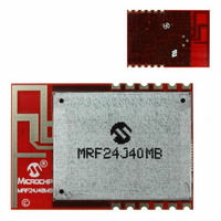
MRF24J40MB-I/RM
Manufacturer Part Number
MRF24J40MB-I/RM
Description
IC TXRX 2.4GHZ 802.15.4
Manufacturer
Microchip Technology
Datasheet
1.MRF24J40MB-IRM.pdf
(34 pages)
Specifications of MRF24J40MB-I/RM
Frequency
2.4GHz
Data Rate - Maximum
250kbps
Modulation Or Protocol
802.15.4
Applications
ISM
Power - Output
20dBm
Sensitivity
-102dBm
Voltage - Supply
2.4V ~ 3.6V
Current - Receiving
25mA
Current - Transmitting
130mA
Data Interface
PCB, Surface Mount
Antenna Connector
On-Board, Trace
Operating Temperature
-40°C ~ 85°C
Package / Case
Module
Wireless Frequency
2.405 GHz to 2.475 GHz
Interface Type
SPI
Security
128 bit AES
Operating Voltage
3.3 V
Output Power
+ 20 dBm
Antenna
PCB Trace
Operating Temperature Range
- 40 C to + 85 C
Modulation Type
O-QPSK
Data Rate Max
250Kbps
Module Interface
SPI, 4-Wire
Supply Voltage Range
2.4V To 3.6V
Sensitivity (dbm)
-102dBm
Supply Current
130mA
Lead Free Status / RoHS Status
Lead free / RoHS Compliant
Memory Size
-
Lead Free Status / Rohs Status
Lead free / RoHS Compliant
Available stocks
Company
Part Number
Manufacturer
Quantity
Price
Company:

Part Number:
MRF24J40MB-I/RM
Manufacturer:
NXP
Quantity:
12 000


1.3
1.3.1
Operation of the Power Amplifier (PA) IC3 and Low Noise
Amplifier (LNA) IC5 is controlled by the MRF24J40
internal RF state machine via RF switches, IC2 and IC4,
and the GPIO1 and GPIO2 pins on the MRF24J40.
Figure 1-6 shows the PA/LNA block diagram. Figure 2-1
is the schematic diagram for the module.
FIGURE 1-6:
1.3.2
Before
Section 3.6.1
Mode 1)” in the “MRF24J40 Data Sheet” (DS39776)),
perform the following steps:
1.
2.
3.
4.
2009 Microchip Technology Inc.
Note:
Configure the internal RF state machine to normal
operation (TESTMODE (0x22F<2:0>) = 000).
Configure GPIO2 and GPIO1 direction for the
output (TRISGP2 (0x34<2>) = 1 and TRISGP1
(0x34<1>) = 1).
Set GPIO2 (0x33<2>) = 1 and GPIO1
(0x32<1>) = 0. This enables the LNA and
disables the PA.
Perform the energy detection following the steps
in Section 3.6.1 “RSSI Firmware Request
(RSSI Mode 1)” in the “MRF24J40 Data Sheet”
(DS39776).
Antenna
PCB
Operation
performing
PA/LNA CONTROL
ENERGY DETECTION (ED)
The LNA will amplify the received signal.
The RSSI value will include the receive
signal strength plus the LNA amplification.
“RSSI
RF Switch
AS179-92
V1 V2
PA/LNA BLOCK DIAGRAM
an
Firmware
energy
LNA
PA
Request
LNA
uPC8233TK
PA
PA2423L
detection
RF Switch
AS179-92
V1 V2
(RSSI
(see
Preliminary
The internal RF state machine is configured for the PA/
LNA mode by setting TESTMODE (0x22F<2:0>) = 111.
Pins, GPIO1 and GPIO2, then control the RF switches,
PA and LNA automatically when the MRF24J40
receives and transmits data.
1.3.3
To get the lowest power consumption from the
MRF24J40MB module during Sleep, it is necessary to
disable both the PA and LNA. To do this, perform the
following steps:
1.
2.
3.
4.
When waking the module, re-enable the PA/LNA mode.
Balun
Note:
Configure the internal RF state machine to normal
operation (TESTMODE (0x22F<2:0>) = 000).
Configure the GPIO2 and GPIO1 direction for
output (TRISGP2 (0x34<2>) = 1 and TRISGP1
(0x34<1>) = 1).
Set
(0x32<1>) = 0. This disables the LNA and the PA.
Put the MRF24J40 to Sleep following the steps
in the “MRF24J40 Data Sheet” (DS39776).
GPIO2 (0x33<2>)
A complete explanation of the operation of
the PA/LNA control is documented in the
“MRF24J40 Data Sheet” (DS39776),
Section 4.2 “External PA/LNA Control”.
SLEEP
MRF24J40MB
GPIO1
GPIO2
RFP
RFN
MRF24J40
= 0
DS70599B-page 7
and
GPIO1
Related parts for MRF24J40MB-I/RM
Image
Part Number
Description
Manufacturer
Datasheet
Request
R

Part Number:
Description:
IC TXRX IEEE/ZIGBEE 2.4GHZ 40QFN
Manufacturer:
Microchip Technology
Datasheet:

Part Number:
Description:
IEEE 802.15.4� 2.4 GHz RF Transceiver
Manufacturer:
MICROCHIP [Microchip Technology]
Datasheet:

Part Number:
Description:
Ieee 802.15.4? 2.4 Ghz Rf Transceiver
Manufacturer:
Microchip Technology Inc.
Datasheet:
Part Number:
Description:
Manufacturer:
Microchip Technology Inc.
Datasheet:
Part Number:
Description:
Manufacturer:
Microchip Technology Inc.
Datasheet:
Part Number:
Description:
Manufacturer:
Microchip Technology Inc.
Datasheet:
Part Number:
Description:
Manufacturer:
Microchip Technology Inc.
Datasheet:
Part Number:
Description:
Manufacturer:
Microchip Technology Inc.
Datasheet:
Part Number:
Description:
Manufacturer:
Microchip Technology Inc.
Datasheet:
Part Number:
Description:
Manufacturer:
Microchip Technology Inc.
Datasheet: