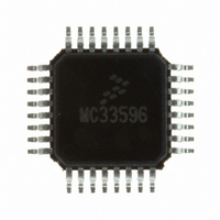
MC33596FJER2 Freescale Semiconductor, MC33596FJER2 Datasheet - Page 46

MC33596FJER2
Manufacturer Part Number
MC33596FJER2
Description
IC RX UHF PLL TUNED 32-LQFP
Manufacturer
Freescale Semiconductor
Datasheet
1.MC33596FCAE.pdf
(70 pages)
Specifications of MC33596FJER2
Frequency
304, 315, 426, 434, 868 & 915MHz
Sensitivity
-104dBm
Data Rate - Maximum
22.4 kBaud
Modulation Or Protocol
FSK, OOK
Applications
General Data Transfer
Current - Receiving
10.3mA
Data Interface
PCB, Surface Mount
Antenna Connector
PCB, Surface Mount
Voltage - Supply
2.7 V ~ 3.6 V, 4.5 V ~ 5.5 V
Operating Temperature
-40°C ~ 85°C
Package / Case
32-LQFP
Operating Temperature (min)
-40C
Operating Temperature (max)
85C
Operating Temperature Classification
Industrial
Modulation Type
FSK/OOK
Package Type
LQFP
Operating Supply Voltage (min)
2.7V
Lead Free Status / RoHS Status
Lead free / RoHS Compliant
Features
-
Memory Size
-
Lead Free Status / Rohs Status
Compliant
Available stocks
Company
Part Number
Manufacturer
Quantity
Price
Part Number:
MC33596FJER2
Manufacturer:
FREESCALE
Quantity:
20 000
Electrical Characteristics
19
19.1 General Parameters
19.2 Receiver: RF Parameters
RF parameters assume a matching network between test equipment and the D.U.T, and apply to all bands
unless otherwise specified.
Operating supply voltage and temperature range see
schematic (see
3.0 V, T
46
Operating supply voltage and temperature range see
schematic (see
3.0 V, T
2.40 OOK sensitivity at 434 MHz DME = 1, DSREF = 1,
2.41 OOK sensitivity at 868 MHz DME = 1, DSREF = 1,
1.12 Receiver on-to-off time
1.13 VCC2 voltage regulator output
1.14
1.15 VCCDIG2 voltage regulator
1.16
1.19 Voltage on VCC (Preregulator
2.2 OOK sensitivity at 315 MHz DME = 1, DSREF = 1,
1.2 Supply current in receive mode
1.3
1.6 Supply current in standby mode –40°C ≤ T
1.8
1.9 Supply current in LVD mode
output
output)
A
A
= 25°C.
= 25°C.
Electrical Characteristics
Parameter
Figure 43
Figure 43
Parameter
through
through
Figure
Figure
DR = 4.8 kbps, PER = 0.1
DR = 4.8 kbps, PER = 0.1
DR = 4.8 kbps, PER = 0.1
Receiver on
Strobe oscillator only
T
LVDE = 1
Supply current reduced to 10%
2.7 V < V
2.1 V ≤ V
Circuit in standby mode
(V
Circuit in all other modes
Receive mode with VCCIN=5V
54), unless otherwise specified. Typical values reflect average measurement at V
54), unless otherwise specified. Typical values reflect average measurement at V
A
CCDIG
= 85°C
Test Conditions,
Comments
Test Conditions
MC33596 Data Sheet, Rev. 4
= 3 V)
CC
CC
A
Comments
≤ 25°C
≤ 2.7 V
Table
Table
3. Values refer to the circuit recommended in the application
3. Values refer to the circuit recommended in the application
Min
—
—
—
Min
2.4
1.4
2.4
—
—
—
—
—
—
—
—
–103.5
–104
–103
Typ
Limits
V
V
Limits
CC
0.7 x
10.3
CCDIG
Typ
260
800
100
2.6
1.6
24
35
—
–0.1
(FCE,
FJE)
Max
–99
–98
–98
Freescale Semiconductor
1200
Max
700
(FCAE,
2.8
1.8
FJAE)
13
50
50
—
—
—
—
Max
–96
–97
–96
Unit
dBm
dBm
dBm
Unit
mA
μA
nA
nA
μA
μs
V
V
V
V
V
CC
CC
=
=


