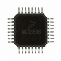
MC33596FJER2 Freescale Semiconductor, MC33596FJER2 Datasheet - Page 40

MC33596FJER2
Manufacturer Part Number
MC33596FJER2
Description
IC RX UHF PLL TUNED 32-LQFP
Manufacturer
Freescale Semiconductor
Datasheet
1.MC33596FCAE.pdf
(70 pages)
Specifications of MC33596FJER2
Frequency
304, 315, 426, 434, 868 & 915MHz
Sensitivity
-104dBm
Data Rate - Maximum
22.4 kBaud
Modulation Or Protocol
FSK, OOK
Applications
General Data Transfer
Current - Receiving
10.3mA
Data Interface
PCB, Surface Mount
Antenna Connector
PCB, Surface Mount
Voltage - Supply
2.7 V ~ 3.6 V, 4.5 V ~ 5.5 V
Operating Temperature
-40°C ~ 85°C
Package / Case
32-LQFP
Operating Temperature (min)
-40C
Operating Temperature (max)
85C
Operating Temperature Classification
Industrial
Modulation Type
FSK/OOK
Package Type
LQFP
Operating Supply Voltage (min)
2.7V
Lead Free Status / RoHS Status
Lead free / RoHS Compliant
Features
-
Memory Size
-
Lead Free Status / Rohs Status
Compliant
Available stocks
Company
Part Number
Manufacturer
Quantity
Price
Part Number:
MC33596FJER2
Manufacturer:
FREESCALE
Quantity:
20 000
Register Description
BANKA defines the register bank selected, as described in
RON[3:0] (Receiver On) define the receiver on time (after crystal oscillator startup) as described in
Section 11.3, “Receiver On/Off
ROFF[2:0] (Receiver Off) define the receiver off time as described in
Control.”
16.5 ID and Header Registers
Figure 30
IDL[1:0] (Identifier Length) sets the length of the identifier, as shown on
40
Reset Value
Bit Name
Access
defines the ID register, ID.
IDL1
Bit 7
R/W
1
IDL0
Bit 6
R/W
1
ROFF[2:0]
RON[3:0]
0000
0001
0010
1111
Control.”
000
001
010
011
100
101
110
111
...
Table 17. Receiver Off Time Definition
Table 16. Receiver On Time Definition
Bit 5
R/W
ID5
0
MC33596 Data Sheet, Rev. 4
Figure 30. ID Register
Receiver On Time: N x 512 x T
Receiver Off Time: N x T
Bit 4
R/W
ID4
0
Forbidden value
Bit 3
R/W
ID3
Section 15, “Configuration
15
12
16
32
63
0
...
1
2
1
2
4
8
Bit 2
R/W
Strobe
ID2
Section 11.3, “Receiver On/Off
0
digclk
Table
18.
Bit 1
R/W
ID1
0
Freescale Semiconductor
Switching.”
Bit 0
R/W
ID0
0
Addr
$0A


