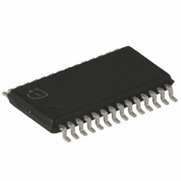
TDA5201 Infineon Technologies, TDA5201 Datasheet - Page 28

TDA5201
Manufacturer Part Number
TDA5201
Description
IC LP SGL CONV ASK P-TSSOP-28
Manufacturer
Infineon Technologies
Type
Receiverr
Datasheet
1.TDA5201.pdf
(38 pages)
Specifications of TDA5201
Package / Case
28-TSSOP
Frequency
310MHz ~ 350MHz
Sensitivity
-107dBm
Modulation Or Protocol
ASK
Applications
Alarm Systems, Communication Systems
Current - Receiving
4.8mA
Data Interface
PCB, Surface Mount
Antenna Connector
PCB, Surface Mount
Voltage - Supply
4.5 V ~ 5.5 V
Operating Temperature
-40°C ~ 85°C
Operating Frequency
350 MHz
Operating Supply Voltage
5 V
Maximum Operating Temperature
+ 125 C
Minimum Operating Temperature
- 40 C
Mounting Style
SMD/SMT
Operating Temperature (min)
-40C
Operating Temperature (max)
125C
Operating Temperature Classification
Automotive
Product Depth (mm)
4.4mm
Product Length (mm)
9.7mm
Operating Supply Voltage (min)
4.5V
Operating Supply Voltage (typ)
5V
Operating Supply Voltage (max)
5.5V
Lead Free Status / RoHS Status
Lead free / RoHS Compliant
Features
-
Memory Size
-
Data Rate - Maximum
-
Lead Free Status / Rohs Status
Compliant
Other names
SP000012902
TDA5201INTR
TDA5201INTR
Available stocks
Company
Part Number
Manufacturer
Quantity
Price
Company:
Part Number:
TDA5201
Manufacturer:
INFINEON
Quantity:
5 510
Company:
Part Number:
TDA5201
Manufacturer:
VISHAY
Quantity:
5 510
Part Number:
TDA5201
Manufacturer:
INFINEON/英飞凌
Quantity:
20 000
Part Number:
TDA5201A3
Manufacturer:
INFINEON/英飞凌
Quantity:
20 000
Company:
Part Number:
TDA5201B1
Manufacturer:
INFINEON
Quantity:
7 007
Part Number:
TDA5201B1
Manufacturer:
INFINEON/英飞凌
Quantity:
20 000
Part Number:
TDA5201B3
Manufacturer:
INFINEON/英飞凌
Quantity:
20 000
Table 6
Parameter
Power Mode Off
Power Mode Off
Gain Control Voltage,
LNA high gain state
Gain Control Voltage,
LNA low gain state
Attention: Test ■ means that the parameter is not subject to production test.
5.1.3
AC/DC characteristics involve the spread of values guaranteed within the specified voltage and ambient
temperature range. Typical characteristics are the median of the production.
Table 7
Parameter
Supply Current
Supply current
standby mode
Supply current
LNA - Signal Input LNI (PIN 3),
Average Power Level
at BER = 2E-3
(Sensitivity)
Input impedance
Input level @ 1 dB C.P.
f
Input 3rd order intercept
point
LO signal feedthrough at
antenna port
LNA - Signal Output LNO (PIN 6),
Gain
Output impedance,
f
Voltage Gain Antenna to
MI
f
RF
RF
Data Sheet
RF
f
= 315 MHz
= 315 MHz
RF
= 315 MHz
f
f
RF
RF
= 315 MHz
= 315 MHz
= 315 MHz
It was verified by design/characterization.
AC/DC Characteristics with
Operating Range, Ambient Temperature
AC/DC Characteristics
Symbol
V
V
V
V
Symbol
I
I
RF
S
P1dB
IIP3
LO
S
S
G
S PDWN
S
11 LNA
OFF
ON
THRES
THRES
21 LNA
22 LNA
AntMI
in
LNI
LNA
LNA
V
THRES
V
Min.
0
2
2.8
0
THRES
Min.
> 3.3 V, High Gain Mode
T
> 3.3 V, High Gain Mode
AMB
Typ.
50
4.6
-113
0.895 /
-25.5 deg
-14
-10
-119
1.577 /
150.3 deg
0.897 /
-10.3 deg
21
Typ.
= 25 °C,
Values
Values
28
T
V
AMB
0.8
V
V
0.7
Max.
CC
CC
CC
Max.
70
5
= 4.5 ... 5.5 V
= - 40 °C ... + 85 °C (cont’d)
-1
Unit
V
V
V
V
Unit
nA
mA
dBm
dBm
dBm
dBm
dB
ASK Single Conversion Receiver
Note /
Test Condition
Note /
Test Condition
Pin 27 (PDWN)
open or tied to 0 V
Manchester
encoded data rate
4 kBit, 280 kHz IF
Bandwidth
f
317 MHz
in
= 315 MHz &
Electrical Characteristics
Revision 1.6, 2010-12-21
Test Number
Test Number
■
■
■
■
■
■
■
■
TDA 5201
2.6
2.7
2.8
2.9
3.1
3.2
3.3
3.4
3.5
3.6
3.7
3.8
3.9
3.10


