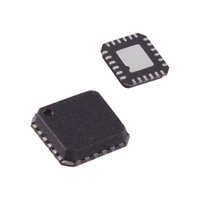
ADL5375-05ACPZ-R7 Analog Devices Inc, ADL5375-05ACPZ-R7 Datasheet - Page 6

ADL5375-05ACPZ-R7
Manufacturer Part Number
ADL5375-05ACPZ-R7
Description
IC MOD QUAD 400MHZ-6GHZ 24LFCSP
Manufacturer
Analog Devices Inc
Datasheet
1.ADL5375-05ACPZ-R7.pdf
(32 pages)
Specifications of ADL5375-05ACPZ-R7
Design Resources
Interfacing ADL5375 to AD9779A Dual-Channel, 1 GSPS High Speed DAC (CN0021) Broadband Low EVM Direct Conversion Transmitter (CN0134)
Function
Modulator
Lo Frequency
400MHz ~ 6GHz
Rf Frequency
400MHz ~ 6GHz
P1db
10.4dBm
Noise Floor
-157.6dBm/Hz
Output Power
1.71dBm
Current - Supply
200mA
Voltage - Supply
4.75 V ~ 5.25 V
Test Frequency
3.5GHz
Package / Case
24-VFQFN, 24-CSP Exposed Pad
Frequency Range
400MHz To 6GHz
Rf Type
Quadrature
Supply Voltage Range
4.75V To 5.25V
Rf Ic Case Style
LFCSP
No. Of Pins
24
Operating Temperature Range
-40°C To +85°C
Frequency Max
6GHz
Lead Free Status / RoHS Status
Lead free / RoHS Compliant
Other names
ADL5375-05ACPZ-R7TR
Available stocks
Company
Part Number
Manufacturer
Quantity
Price
Part Number:
ADL5375-05ACPZ-R7
Manufacturer:
ADI/亚德诺
Quantity:
20 000
ADL5375
Parameter
LO = 5800 MHz
LO INPUTS
BASEBAND INPUTS
OUTPUT DISABLE
POWER SUPPLIES
1
The input bias level can vary as long as the voltages on the individual IBBP, IBBN, QBBP, and QBBN pins remain within the specified absolute voltage level.
Output Power, P
Modulator Voltage Gain
Output P1dB
Output Return Loss
Carrier Feedthrough
Sideband Suppression
Quadrature Error
I/Q Amplitude Balance
Second Harmonic
Third Harmonic
Output IP2
Output IP3
Noise Floor
LO Drive Level
Input Return Loss
I/Q Input Bias Level
Absolute Voltage Level
Input Bias Current
Input Offset Current
Differential Input
Impedance
Bandwidth (0.1 dB)
Off Isolation
Turn-On Settling Time
Turn-Off Settling Time
DSOP High Level (Logic 1)
DSOP Low Level (Logic 0)
Voltage
Supply Current
ADL5375-05
ADL5375-15
ADL5375-05
ADL5375-15
OUT
1
1
Conditions
V
RF output divided by baseband input voltage
P
P
f1
P
f1
P
I/Q inputs = 0 V differential with a dc bias
only, 20 MHz carrier offset
Characterization performed at typical level
500 MHz < f
See Figure 7 and Figure 32 for return loss vs.
frequency
Pin IBBP, Pin IBBN, Pin QBBP, Pin QBBN
On Pin IBBP, Pin IBBN, Pin QBBP, Pin QBBN
LO = 1900 MHz, baseband input =
500 mV p-p sine wave
Pin DSOP
DSOP low, LO leakage, LO = 2150 MHz
DSOP high to low (90% of envelope)
DSOP low to high (10% of envelope)
Pin VPS1 and Pin VPS2
DSOP = high
DSOP = low
P
P
P
P
Current sourcing from each baseband input
P
IQ
OUT
OUT
OUT
OUT
OUT
OUT
OUT
OUT
OUT
BB
BB
= 1 V p-p differential
= 3.5 MHz, f2
= 3.5 MHz, f2
− (f
− (f
≈ −5 dBm @ f
≈ −5 dBm @ f
(DSOP high) – P
= 2.40 dBm
= 0.82 dBm
= 2.40 dBm
= 0.82 dBm
LO
LO
+ (2 × f
+ (3 × f
LO
< 3.3 GHz
BB
BB
BB
BB
LO
LO
))
))
= 4.5 MHz,
= 4.5 MHz,
= 900 MHz
= 900 MHz
OUT
(DSOP low)
Rev. A | Page 6 of 32
Min
−6
0
2.0
4.75
ADL5375-05
Typ
2.40
−1.6
5.7
−11.4
−23.0
−36.0
−1.42
0.20
−57
−43
38.7
13.5
−153.0
0
≤−10
500
41
0.1
60
95
86
−53
200
100
200
131
Max
+7
1
0.8
5.25
Min
2.0
4.75
−6
1
ADL5375-15
Typ
0.82
−3.2
6.6
−10.5
−16.3
−33.0
+1.17
0.50
−58
−52
35.7
12.1
−153.4
0
≤−10
1500
32
0.1
100
80
85
−53
200
100
200
131
Max
+7
2
0.8
5.25
Unit
dBm
dB
dBm
dB
dBm
dBc
Degrees
dB
dBc
dBc
dBm
dBm
dBm/Hz
dBm
dB
mV
V
μA
μA
kΩ
MHz
dB
dBm
ns
ns
V
V
V
mA
mA


