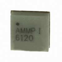
AMMP-6120-BLK Avago Technologies US Inc., AMMP-6120-BLK Datasheet - Page 6

AMMP-6120-BLK
Manufacturer Part Number
AMMP-6120-BLK
Description
8-24 GHZ FREQ MULTIPLIER X2 SMD
Manufacturer
Avago Technologies US Inc.
Datasheet
1.AMMP-6120-BLK.pdf
(9 pages)
Specifications of AMMP-6120-BLK
Function
Frequency Multiplier
Frequency
4GHz ~ 12GHz
Rf Type
VSAT, DBS
Secondary Attributes
Output Power -11 to 5dBm
Package / Case
8-QFN
Supply Current
85mA
Supply Voltage Range
5V
Rf Ic Case Style
SMD
No. Of Pins
8
Frequency Max
24GHz
Termination Type
SMD
Frequency Min
8GHz
Supply Voltage Max
7V
Gain
1dB
Operating Temperature Max
150°C
Rohs Compliant
Yes
Filter Terminals
SMD
Lead Free Status / RoHS Status
Lead free / RoHS Compliant
Other names
516-1853
AMMP-6120-BLK
Q2313336
AMMP-6120-BLK
Q2313336
Available stocks
Company
Part Number
Manufacturer
Quantity
Price
Company:
Part Number:
AMMP-6120-BLK
Manufacturer:
SYNERGY
Quantity:
5 000
Part Number:
AMMP-6120-BLK
Manufacturer:
AVAGO/安华高
Quantity:
20 000
Figure. 19 2H Output Power Vs Input Power @ Fout=26GHz
Figure.21 SSB Phase Noise of frequency doubler
(Pin=+2dBm, fout=15.6GHz)
Biasing and Operation
The frequency doubler MMIC consists of a balun. The
outputs of this balun feed the gates of balanced FETs and
the drains are connected to form the single-ended output.
This results in fundamental frequency & odd harmonics
cancellation. The even harmonic drain currents are in
phase and thus add in phase. The input matching network
(M/N) is designed to provide good match at fundamental
frequencies and produces high impedance mismatch to
higher harmonics.
The AMMP-6120 is biased with a single positive drain
supply Vdd and a single negative gate supply using
separate bypass capacitors. It is normally biased with
the drain supply connected to Vd and the gate supply
connected to Vg. For most applications it is recommended
to use a Vg =-1.2V to -1.4V and Vd=4.5V to 5.0V.
The RF input and output ports are AC coupled thus no DC
voltage is present at either port. The ground connection is
made via the package base. ”
6
-100
-110
-120
-130
-140
-150
-160
-170
20
18
16
14
12
10
-50
-60
-70
-80
-90
8
6
4
2
0
1.E+02
-11 -9
Fout=26GHz
Vd=4.5V, Vg=-1.2V
-7
1.E+03
Input Power [1H] (dBm)
-5
-3
Offset Frequency [Hz]
1.E+04
-1
1
1.E+05
Vg=-1.2V, Vd=4.5V
Vg=-1.2V, Vd=5.0V
Vg=-1.4V, Vd=4.5V
Vg=-1.4V, Vd=5.0V
3
Fout=15.6GHz
5
1.E+06
7
9
1.E+07
11
Figure. 20 Fundamental Supp. Vs Input Power @ Fout=26GHz
Figure 22. Top Level Schematic of Frequency doubler
The AMMP-6120 performance changes with Drain Voltage
(Vd) and Gate bias (Vg) as shown in the previous graphs.
Improvements in output power or fundamental suppres-
sion performance are possible by optimizing the Vg from
-1.2V to -1.4V and/or Vd from 4.5 to 5.0V.
A simplified schematic of the frequency multiplier is
shown in figure 22. The active balun circuit and the output
amplifier of the circuit are self biased. The Vg negative bias
(below pinch off ) is only applied to FETs ‘F1’ and ‘F2’ . FETs
‘F1’ and ‘F2’ have no significant contribution to total drain
current therefore Vg cannot be used to set drain current.
It should only be used to optimize the output power
and fundamental & higher harmonics suppression of the
doubler.
Refer to the Absolute Maximum Ratings table for allowed
DC and thermal conditions.
35
10
15
20
25
30
5
-11
M/N
@ fo
-9
-7
Active
Balun
-5
Input Power [1H] (dBm)
Fout=26GHz
-3
-1
Vg=-1.2V, Vd=4.5V
Vg=-1.2V, Vd=5.0V
Vg=-1.4V, Vd=4.5V
Vg=-1.4V, Vd=5.0V
F1
F2
1
S
3
5
@ 2fo
Filter
7
9
Amp
11


