AD6655-125EBZ Analog Devices Inc, AD6655-125EBZ Datasheet - Page 2
AD6655-125EBZ
Manufacturer Part Number
AD6655-125EBZ
Description
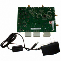
BOARD EVAL W/AD6655 & SOFTWARE
Manufacturer
Analog Devices Inc
Type
Receiver, CDMAr
Specifications of AD6655-125EBZ
Frequency
450MHz
Silicon Manufacturer
Analog Devices
Application Sub Type
IF Diversity Receiver
Kit Application Type
Communication & Networking
Silicon Core Number
AD6655
Kit Contents
Evaluation Board With AD6655 And Software
Lead Free Status / RoHS Status
Lead free / RoHS Compliant
For Use With/related Products
AD6655
Lead Free Status / Rohs Status
Compliant


AD6655
TABLE OF CONTENTS
Features .............................................................................................. 1
Applications ....................................................................................... 1
Product Highlights ........................................................................... 1
Functional Block Diagram .............................................................. 1
Revision History ............................................................................... 3
General Description ......................................................................... 4
Specifications ..................................................................................... 5
Absolute Maximum Ratings .......................................................... 18
Pin Configurations and Function Descriptions ......................... 19
Equivalent Circuits ......................................................................... 23
Typical Performance Characteristics ........................................... 24
Theory of Operation ...................................................................... 29
Digital Downconverter .................................................................. 37
ADC DC Specifications—AD6655BCPZ-80/
AD6655BCPZ-105 ......................................................................... 5
ADC DC Specifications—AD6655BCPZ-125/
AD6655BCPZ-150 ......................................................................... 6
ADC AC Specifications—AD6655BCPZ-80/
AD6655BCPZ-105 ......................................................................... 7
ADC AC Specifications—AD6655BCPZ-125/
AD6655BCPZ-150 ......................................................................... 8
Digital Specifications—AD6655BCPZ-80/AD6655BCPZ-105 .. 9
Digital Specifications—AD6655BCPZ-125/
AD6655BCPZ-150 ....................................................................... 11
Switching Specifications—AD6655BCPZ-80/
AD6655BCPZ-105 ....................................................................... 13
Switching Specifications—AD6655BCPZ-125/
AD6655BCPZ-150 ....................................................................... 14
Timing Specifications ................................................................ 15
Thermal Characteristics ............................................................ 18
ESD Caution ................................................................................ 18
ADC Architecture ...................................................................... 29
Analog Input Considerations .................................................... 29
Voltage Reference ....................................................................... 31
Clock Input Considerations ...................................................... 32
Power Dissipation and Standby Mode ..................................... 34
Digital Outputs ........................................................................... 35
Downconverter Modes .............................................................. 37
Numerically Controlled Oscillator (NCO) ............................. 37
Half-Band Decimating Filter and FIR Filter ........................... 37
f
ADC
/8 Fixed-Frequency NCO ................................................... 37
Rev. A | Page 2 of 88
Numerically Controlled Oscillator (NCO) ................................. 38
Decimating Half-Band Filter and FIR filter ................................ 39
ADC Overrange and Gain Control .............................................. 41
Signal Monitor ................................................................................ 44
Channel/Chip Synchronization .................................................... 47
Serial Port Interface (SPI) .............................................................. 48
Memory Map .................................................................................. 50
Applications Information .............................................................. 59
Evaluation Board ............................................................................ 61
Frequency Translation ............................................................... 38
NCO Synchronization ............................................................... 38
Phase Offset................................................................................. 38
NCO Amplitude and Phase Dither .......................................... 38
Half-Band Filter Coefficients .................................................... 39
Half-Band Filter Features .......................................................... 39
Fixed-Coefficient FIR Filter ...................................................... 39
Synchronization .......................................................................... 40
Combined Filter Performance .................................................. 40
Final NCO ................................................................................... 40
Fast Detect Overview ................................................................. 41
ADC Fast Magnitude ................................................................. 41
ADC Overrange (OR) ................................................................ 42
Gain Switching ............................................................................ 42
Peak Detector Mode................................................................... 44
RMS/MS Magnitude Mode ....................................................... 44
Threshold Crossing Mode ......................................................... 45
Additional Control Bits ............................................................. 45
DC Correction ............................................................................ 45
Signal Monitor SPORT Output ................................................ 46
Configuration Using the SPI ..................................................... 48
Hardware Interface ..................................................................... 48
Configuration Without the SPI ................................................ 49
SPI Accessible Features .............................................................. 49
Reading the Memory Map Register Table ............................... 50
Memory Map Register Table ..................................................... 51
Memory Map Register Description ......................................... 55
Design Guidelines ...................................................................... 59
Power Supplies ............................................................................ 61
Input Signals................................................................................ 61
Related parts for AD6655-125EBZ
Image
Part Number
Description
Manufacturer
Datasheet
Request
R

Part Number:
Description:
BOARD EVAL FOR 150MSPS AD6655
Manufacturer:
Analog Devices Inc
Datasheet:

Part Number:
Description:
±1.7g Dual-Axis IMEMS Accelerometer Evaluation Board
Manufacturer:
Analog Devices Inc
Datasheet:

Part Number:
Description:
Inertial Sensor Evaluation System
Manufacturer:
Analog Devices Inc
Datasheet:
Part Number:
Description:
Manufacturer:
Analog Devices Inc
Datasheet:
Part Number:
Description:
Manufacturer:
Analog Devices Inc
Datasheet:
Part Number:
Description:
Manufacturer:
Analog Devices Inc
Datasheet:
Part Number:
Description:
Manufacturer:
Analog Devices Inc
Datasheet:
Part Number:
Description:
Manufacturer:
Analog Devices Inc
Datasheet:
Part Number:
Description:
Manufacturer:
Analog Devices Inc
Datasheet:
Part Number:
Description:
Manufacturer:
Analog Devices Inc
Datasheet:
Part Number:
Description:
Manufacturer:
Analog Devices Inc
Datasheet:
Part Number:
Description:
Manufacturer:
Analog Devices Inc
Datasheet:
Part Number:
Description:
Manufacturer:
Analog Devices Inc
Datasheet: