1000-TCB1C470 Silicon Laboratories Inc, 1000-TCB1C470 Datasheet - Page 17
1000-TCB1C470
Manufacturer Part Number
1000-TCB1C470
Description
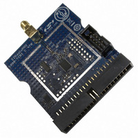
BOARD EVALUATION FOR SI1000
Manufacturer
Silicon Laboratories Inc
Type
Transceiver, ISMr
Specifications of 1000-TCB1C470
Mfg Application Notes
SI1000 Code Examples AppNote
Frequency
470MHz
Supply Voltage (min)
0.9 V
Product
RF Modules
Maximum Frequency
915 MHz
Output Power
20 dBm
Antenna
SMA
Supply Voltage (max)
3.6 V
For Use With/related Products
Si100x
Lead Free Status / RoHS Status
Lead free / RoHS Compliant
Lead Free Status / RoHS Status
Lead free / RoHS Compliant, Lead free / RoHS Compliant
Other names
336-1893


10.5. Switches and LEDs
Three push-button switches are provided on the target board. Switch SW1 is connected to the reset pin of the
MCU. Pressing SW1 puts the device into its hardware-reset state. Switches SW2 and SW3 are connected to the
MCU’s general purpose I/O (GPIO) pins through headers. Pressing SW2 or SW3 generates a logic low signal on
the port pin. Remove the shorting block from the header (J8) to disconnect the switches from the port pins. The
port pin signal is also routed to pins on the J2 and P1 I/O connectors. See Table 1 for the port pins and headers
corresponding to each switch.
Two touch sensitive (contactless) switches are provided on the target board. The operation of these switches
require appropriate firmware running on the Si10xx MCU that can sense the state of the switch.
Five power LEDs are provided on the target board to serve as indicators. Each of the two regulators has a red LED
used to indicate the presence of power at the output of the regulator. A red USB Power LED turns on when a USB
cable is plugged into the USB connector P3. One power LED is also added to each of the two primary supply nets
powering the MCU (VDD/DC+ and VBAT). The LEDs connected to the supply nets may be disabled by removing
the shorting blocks from J1 and J5.
Two LEDs are connected to GPIO pins P1.5 and P1.6 for use by application software. See Table 1 for the port pins
and headers corresponding to each LED.
A potentiometer (R15) is also provided on the target board for generating analog signals. Place a shorting block on
J16 to connect the wiper to P0.6/CNVSTR. The header J15 allows the negative terminal of the potentiometer to be
tied to GND or to P2.7. When tied to GND, the potentiometer is always enabled and will draw a measurable
amount of supply current. When tied to P2.7, it only draws current when P2.7 is driving a logic 0 and draws no
current when P2.7 is driving a logic 1.
P0.6 (Touch Sense Switch)
Red LED (+1 VD Power)
Red LED (+3 VD Power)
Red LED (USB Power)
Red LED (VDD/DC+)
Potentiometer (R15)
Yellow LED (P1.6)
Red LED (VBAT)
Red LED (P1.5)
Description
SW1
SW2
SW3
Table 1. Target Board I/O Descriptions
+1 VD Regulator Output
+3 VD Regulator Output
VDD/DC+ Supply Net
Rev. 0.1
VBAT Supply Net
USB VBUS
P0.6/P2.7
Reset
P0.2
P0.3
P0.6
P1.5
P1.6
I/O
Header(s)
J15, J16
J8[5–6]
J8[7–8]
J8[1–2]
J8[3–4]
none
none
none
none
none
J5
J1
Si10xx-DK
17
Related parts for 1000-TCB1C470
Image
Part Number
Description
Manufacturer
Datasheet
Request
R


Part Number:
Description:
BOARD EVALUATION FOR SI1000
Manufacturer:
Silicon Laboratories Inc
Datasheet:

Part Number:
Description:
Industrial Pressure Sensors Force Sensor 20mV/V 1000 lbf Compression
Manufacturer:
Measurement Specialties Inc.
Datasheet:

Part Number:
Description:
MODULE NETWORK 915MHZ
Manufacturer:
Helicomm Inc
Datasheet:

Part Number:
Description:
Transformers Auto 230V/115V
Manufacturer:
Stancor
Datasheet:
Part Number:
Description:
Transformers Isolation 230V/115V
Manufacturer:
Stancor
Datasheet:
Part Number:
Description:
Transformers Isolation 115V/115V
Manufacturer:
Stancor
Datasheet:

Part Number:
Description:
1000 FT SPOOL, PTFE COVERED WIRE
Manufacturer:
NEWPORT ELECTRONICS

Part Number:
Description:
1000' STRANDED CAT5E CABLE (YELLOW),ROHS
Manufacturer:
BELKIN

Part Number:
Description:
SMD/C�/SINGLE-ENDED OUTPUT SILICON OSCILLATOR
Manufacturer:
Silicon Laboratories Inc
Part Number:
Description:
Manufacturer:
Silicon Laboratories Inc
Datasheet:
Part Number:
Description:
N/A N/A/SI4010 AES KEYFOB DEMO WITH LCD RX
Manufacturer:
Silicon Laboratories Inc
Datasheet:
Part Number:
Description:
N/A N/A/SI4010 SIMPLIFIED KEY FOB DEMO WITH LED RX
Manufacturer:
Silicon Laboratories Inc
Datasheet: