ATAB5428-8-WB Atmel, ATAB5428-8-WB Datasheet - Page 96
ATAB5428-8-WB
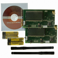
Manufacturer Part Number
ATAB5428-8-WB
Description
KIT DEMO 868MHZ BLACKBIRD
Manufacturer
Atmel
Series
Smart RFr
Type
Transceiver, UHFr
Specifications of ATAB5428-8-WB
Frequency
868MHz
Maximum Frequency
868 MHz
Output Power
0 dBm to 10 dBm
Supply Voltage (max)
6 V
Supply Voltage (min)
3 V
Supply Current
21 mA
Maximum Operating Temperature
+ 85 C
Board Size
2 in x 3.5 in
Minimum Operating Temperature
- 40 C
Product
RF Modules
For Use With/related Products
ATA5428
Lead Free Status / RoHS Status
Lead free / RoHS Compliant
Other names
ATAB-5428-8-WB


17. Digital Port Characteristics (Continued)
All parameters refer to GND and are valid for T
V
V
96
*) Type means: A = 100% tested, B = 100% correlation tested, C = Characterized on samples, D = Design parameter
Note:
VS2
VS1
17.10
17.11
17.12
17.13
17.14
17.15
17.9
No.
= 4.4V to 6.6 V (2
= V
VS2
1. If a logic high level is applied to this pin, a minimum serial impedance of 100 must be ensured for proper operation over full
Parameters
PWR_H input
Low level input voltage
Input current low
High level input voltage
Input current high
SDO_TMDO output
Saturation voltage low
Saturation voltage high
IRQ output
Saturation voltage low
Saturation voltage high
CLK output
Saturation voltage low
Saturation voltage high
N_RESET output
Saturation voltage low
Saturation voltage high
RX_ACTIVE output
Saturation voltage low
Saturation voltage high
DEM_OUT output
Saturation voltage low
ATA5423/ATA5425/ATA5428/ATA5429
= 3V and T
temperature range.
amb
Li b
= 25°C unless otherwise specified.
attery application (6V)) and V
Test Conditions
V
I
V
I
V
I
V
I
V
I
internal series resistor
of 1 k for spurious
emission reduction in
PLL
V
I
internal series resistor
of 1 k for spurious
emission reduction in
PLL
V
I
V
I
V
I
V
I
Open drain output
I
SDO_TMDO
SDO_TMDO
IRQ
IRQ
CLK
CLK
N_RESET
N_RESET
RX_ACTIVE
RX_ACTIVE
DEM_OUT
VSINT
VSINT
VSINT
VSINT
VSINT
VSINT
VSINT
VSINT
VSINT
VSINT
= 250 µA
=
= 100 µA
=
–
–
= 2.4V to 5.25V
= 2.4V to 5.25V
= 2.4V to 5.25V
= 2.4V to 5.25V
= 2.4V to 5.25V
= 2.4V to 5.25V
= 2.4V to 5.25V
= 2.4V to 5.25V
= 2.4V to 5.25V
= 2.4V to 5.25V
250 µA
100 µA
= 250 µA
=
= 250 µA
= 25 µA
=
= 250 µA
=
–
amb
250 µA
–
–
1500 µA
250 µA
=
–
40°C to +85 °C, V
VS2
= 4.75V to 5.25V (Base
Pin
31
31
29
29
30
30
28
28
46
46
34
9
9
9
9
VS1
Symbol
V
V
V
V
V
V
V
V
V
V
V
V
V
I
I
= V
Ih
oh
oh
oh
oh
oh
Il
Ih
ol
ol
ol
ol
ol
ol
Il
S2
= 2.4V to 3.6V (1
-
V
V
V
V
station Application (5V)). Typical values at
V
VSINT
VSINT
VSINT
VSINT
Min.
–
1.7
0.4
0.4
0.4
0.4
AVCC
0.5
–
–
–
–
V
V
V
V
V
–
VSINT
VSINT
VSINT
VSINT
Typ.
0.15
0.15
0.15
0.15
0.15
0.15
0.15
0.15
0.25
0.15
AVCC
0.15
Li b
–
–
–
–
attery application (3V)) and
AVCC
Max.
0.25
0.4
0.4
0.4
0.4
0.4
0.4
–
1
5
Unit
µA
µA
V
V
V
V
V
V
V
V
V
V
V
V
V
4841D–WIRE–10/07
Type*
A
A
A
A
B
B
B
B
B
B
B
B
B
B
B
Related parts for ATAB5428-8-WB
Image
Part Number
Description
Manufacturer
Datasheet
Request
R


Part Number:
Description:
KIT DEMO 434MHZ BLACKBIRD
Manufacturer:
Atmel
Datasheet:

Part Number:
Description:
BOARD BASESTATN UHF RCVR 433MHZ
Manufacturer:
Atmel
Datasheet:
Part Number:
Description:
BOARD BASESTATN UHF RCVR 868MHZ
Manufacturer:
Atmel
Datasheet:

Part Number:
Description:
DEV KIT FOR AVR/AVR32
Manufacturer:
Atmel
Datasheet:

Part Number:
Description:
INTERVAL AND WIPE/WASH WIPER CONTROL IC WITH DELAY
Manufacturer:
ATMEL Corporation
Datasheet:
Part Number:
Description:
Low-Voltage Voice-Switched IC for Hands-Free Operation
Manufacturer:
ATMEL Corporation
Datasheet:
Part Number:
Description:
MONOLITHIC INTEGRATED FEATUREPHONE CIRCUIT
Manufacturer:
ATMEL Corporation
Datasheet:
Part Number:
Description:
AM-FM Receiver IC U4255BM-M
Manufacturer:
ATMEL Corporation
Datasheet:
Part Number:
Description:
Monolithic Integrated Feature Phone Circuit
Manufacturer:
ATMEL Corporation
Datasheet:
Part Number:
Description:
Multistandard Video-IF and Quasi Parallel Sound Processing
Manufacturer:
ATMEL Corporation
Datasheet:
Part Number:
Description:
High-performance EE PLD
Manufacturer:
ATMEL Corporation
Datasheet: