MICRF505DEV1 Micrel Inc, MICRF505DEV1 Datasheet - Page 10
MICRF505DEV1
Manufacturer Part Number
MICRF505DEV1
Description
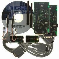
KIT DEV RADIOWIRE 850-950MHZ
Manufacturer
Micrel Inc
Series
RadioWire®r
Type
Transceiver, ISMr
Specifications of MICRF505DEV1
Frequency
850MHz ~ 950MHz
For Use With/related Products
MICRF505
Lead Free Status / RoHS Status
Lead free / RoHS Compliant
Other names
576-1606
Available stocks
Company
Part Number
Manufacturer
Quantity
Price
Company:

Part Number:
MICRF505DEV1
Manufacturer:
Micrel Inc
Quantity:
135


Writing to the control registers in MICRF505
Writing: A number of octets are entered into
MICRF505 followed by a load-signal to activate the
new setting. Making these events is referred to as a
“write sequence.” It is possible to update all, 1, or n
control registers in a write sequence. The address to
write to (or the first address to write to) can be any
valid address (0-21). The IO line is always an input
to the MICRF505 (output from user) when writing.
What to write:
What to write:
Field
Address:
R/W bit:
Values:
How to write:
Bring CS active to active to start a write sequence.
The active state of the CS line is “high.” Use the
SCLK/IO serial interface to clock “Address” and
“R/W” bit and “Values” into the MICRF505.
MICRF505 will sample the IO line at negative edges
of SCLK. Make sure to change the state of the IO
line before the negative edge. Refer to figures
below.
Bring CS inactive to make an internal load-signal
and complete the write-sequence. Note: there is an
exception to this point. If the programming bit called
“load_en” (bit0 in ControlRegister0) is “0”, then no
load pulse is generated.
October 2006
•
•
•
The address of the control register to be
written (or if more than 1 control register
should be written to, the address of the 1
control register to write to).
A bit to enable reading or writing of the
control registers. This bit is called the R/W
bit.
The values
register(s).
Comments
A 7-bit field, ranging from 0 to 21. MSB is
written first.
A 1-bit field, = “0” for writing
A number of octets (1-22 octets). MSB in
every octet is written first. The first octet is
written to the control register with the
specified address (=”Address”). The next
octet (if there is one) is written to the control
register with address = “Address + 1” and so
on.
Table 2.
to
write into the control
st
10
The two different ways to “program the chip” are:
Writing to a Single Register
Writing to a control register with address “A6. A5,
…A0” is described here. During operation, writing to
1 register is sufficient to change the way the
transceiver works. Typical example: Change from
receive mode to power-down.
What to write:
Field
Address:
R/W bit:
Values:
“Address” and “R/W bit” together make 1 octet.
In addition, 1 octet with programming bits is entered. In
total, 2 octets are clocked into the MICRF505.
How to write:
CS
In Figure 1, IO is changed at positive edges of SCLK. The
MICRF505 samples the IO line at negative edges. The
value of the R/W bits is always “0” for writing.
SCLK
IO
•
•
•
•
•
Write to a number of control registers (0-22)
when
addresses (write to 1, all or n registers)
Write to a number of control registers when
the
addresses.
Bring CS high
Use SCLK and IO to clock in the 2 octets
Bring CS low
A6
Address of register i
Comments
7 bit = A6, A5, …A0 (A6 = msb. A0 = lsb)
“0” for writing
8 bits = D7, D6, …D0 (D7 = msb, D0 = lsb)
A5
registers
the
A0
registers
Figure 1.
Table 3.
RW
RW
have
D7
Data to write into register i
Internal load pulse made here
have
D6
+1 408-944-0800
non-incremental
M9999-103106
incremental
D2
D1
D0
Related parts for MICRF505DEV1
Image
Part Number
Description
Manufacturer
Datasheet
Request
R

Part Number:
Description:
Manufacturer:
Micrel Inc
Datasheet:
Part Number:
Description:
Manufacturer:
Micrel Inc
Datasheet:
Part Number:
Description:
Manufacturer:
Micrel Inc
Datasheet:
Part Number:
Description:
Manufacturer:
Micrel Inc
Datasheet:
Part Number:
Description:
Manufacturer:
Micrel Inc
Datasheet:
Part Number:
Description:
Manufacturer:
Micrel Inc
Datasheet:
Part Number:
Description:
Manufacturer:
Micrel Inc
Datasheet:
Part Number:
Description:
Manufacturer:
Micrel Inc
Datasheet:
Part Number:
Description:
Manufacturer:
Micrel Inc
Datasheet:
Part Number:
Description:
Manufacturer:
Micrel Inc
Datasheet:
Part Number:
Description:
Manufacturer:
Micrel Inc
Datasheet:
Part Number:
Description:
Manufacturer:
Micrel Inc
Datasheet:
Part Number:
Description:
Manufacturer:
Micrel Inc
Datasheet:
Part Number:
Description:
Manufacturer:
Micrel Inc
Datasheet: