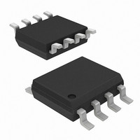
AD8314ARMZ Analog Devices Inc, AD8314ARMZ Datasheet - Page 16

AD8314ARMZ
Manufacturer Part Number
AD8314ARMZ
Description
IC RF DETECTOR/CTRLR 8-MSOP
Manufacturer
Analog Devices Inc
Datasheet
1.AD8314ACPZ-RL7.pdf
(20 pages)
Specifications of AD8314ARMZ
Rf Type
Cellular, GSM, TDMA, CDMA
Frequency
100MHz ~ 2.7GHz
Input Range
-45dBm ~ 0dBm
Voltage - Supply
2.7 V ~ 5.5 V
Current - Supply
5.7mA
Package / Case
8-TSSOP, 8-MSOP (0.118", 3.00mm Width)
Frequency Range
100MHz To 2.7GHz
Supply Current
4.5mA
Supply Voltage Range
2.7V To 5.5V
Rf Ic Case Style
MSOP
No. Of Pins
8
Lead Free Status / RoHS Status
Lead free / RoHS Compliant
Accuracy
-
Lead Free Status / RoHS Status
Lead free / RoHS Compliant, Lead free / RoHS Compliant
Available stocks
Company
Part Number
Manufacturer
Quantity
Price
Company:
Part Number:
AD8314ARMZ
Manufacturer:
AD
Quantity:
5 510
Company:
Part Number:
AD8314ARMZ
Manufacturer:
AD
Quantity:
2 197
Part Number:
AD8314ARMZ
Manufacturer:
ADI/亚德诺
Quantity:
20 000
Company:
Part Number:
AD8314ARMZ-REEL7
Manufacturer:
AD
Quantity:
1 168
Company:
Part Number:
AD8314ARMZ-REEL7
Manufacturer:
ADI44
Quantity:
132
Part Number:
AD8314ARMZ-REEL7
Manufacturer:
ADI/亚德诺
Quantity:
20 000
AD8314
MOBILE HANDSET POWER CONTROL EXAMPLES
Figure 39 shows a complete power amplifier control circuit for a
dual mode handset. This circuit is applicable to any dual mode
handset using TDMA or CDMA technologies. The PF08107B
(Hitachi) is driven by a nominal power level of 3 dBm. Some of
the output power from the PA is coupled off using an
LDC15D190A0007A (Murata) directional coupler. This has a
coupling factor of approximately 19 dB for its lower frequency
band (897.5 MHz ± 17.5 MHz) and 14 dB for its upper band
(1747.5 MHz ± 37.5 MHz) and an insertion loss of 0.38 dB
and 0.45 dB, respectively. Because the PF08107B transmits a
maximum power level of 35 dBm, additional attenuation of
15 dB is required before the coupled signal is applied to
the AD8314.
0V TO 1.1V
ANTENNA
ATTN
VSET
15dB
TO
Figure 39. A Dual Mode Power Amplifier Control Circuit
LDC15D190A0007A
0dBm
MAX
52.3Ω
V
7
8
5
S
2
1
2
3
4
6
1
4
3
RFIN
ENBL
VSET
FLTR
AD8314
49.9Ω
220pF
POUT BAND 1
POUT BAND 2
32dBm MAX
C
35dBm MAX
F
COMM
VPOS
V_DN
V_UP
8
7
6
5
PF08107B
(HITACHI)
SELECT
1000pF
4.7µF
BAND
0V/2V
3.5V
0.1µF
V
V
CTL
APC
V
2.7V
S
PIN BAND 1
3dBm
PIN BAND 2
3dBm
Rev. B | Page 16 of 20
The setpoint voltage, in the 0 V to 1.1 V range, is applied to the
VSET pin of the AD8314. This is typically supplied by a DAC.
This voltage is compared to the input level of the AD8314. Any
imbalance between VSET and the RF input level is corrected by
V_DN, which drives the V
amplifier. V_DN reaches a maximum value of approximately
1.9 V on a 2.7 V supply (this is higher for higher supply
voltages) while delivering approximately 3 mA to the V
A filter capacitor (C
choice of C
dynamics of the power amplifier, something that is frequently
characterized poorly, so some trial and error can be necessary.
In this example, a 220 pF capacitor gives the loop sufficient
speed to follow the GSM and DCS1800 time slot ramping
profiles, while still having a stable, critically damped response.
F
depends to a large degree on the gain control
F
) must be used to stabilize the loop. The
APC
(gain control) of the power
APC
input.


