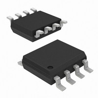
AD8314ARMZ Analog Devices Inc, AD8314ARMZ Datasheet - Page 11

AD8314ARMZ
Manufacturer Part Number
AD8314ARMZ
Description
IC RF DETECTOR/CTRLR 8-MSOP
Manufacturer
Analog Devices Inc
Datasheet
1.AD8314ACPZ-RL7.pdf
(20 pages)
Specifications of AD8314ARMZ
Rf Type
Cellular, GSM, TDMA, CDMA
Frequency
100MHz ~ 2.7GHz
Input Range
-45dBm ~ 0dBm
Voltage - Supply
2.7 V ~ 5.5 V
Current - Supply
5.7mA
Package / Case
8-TSSOP, 8-MSOP (0.118", 3.00mm Width)
Frequency Range
100MHz To 2.7GHz
Supply Current
4.5mA
Supply Voltage Range
2.7V To 5.5V
Rf Ic Case Style
MSOP
No. Of Pins
8
Lead Free Status / RoHS Status
Lead free / RoHS Compliant
Accuracy
-
Lead Free Status / RoHS Status
Lead free / RoHS Compliant, Lead free / RoHS Compliant
Available stocks
Company
Part Number
Manufacturer
Quantity
Price
Company:
Part Number:
AD8314ARMZ
Manufacturer:
AD
Quantity:
5 510
Company:
Part Number:
AD8314ARMZ
Manufacturer:
AD
Quantity:
2 197
Part Number:
AD8314ARMZ
Manufacturer:
ADI/亚德诺
Quantity:
20 000
Company:
Part Number:
AD8314ARMZ-REEL7
Manufacturer:
AD
Quantity:
1 168
Company:
Part Number:
AD8314ARMZ-REEL7
Manufacturer:
ADI44
Quantity:
132
Part Number:
AD8314ARMZ-REEL7
Manufacturer:
ADI/亚德诺
Quantity:
20 000
Table 4. Typical Specifications at Selected Frequencies at 25°C (Mean and Σ)
Frequency (GHz)
0.1
0.9
1.9
2.5
1
However, the logarithmic slope, the amount by which the
output V_UP changes for each decibel of input change (voltage
or power) is, in principle, independent of waveform or termination
impedance. In practice, it usually falls off somewhat at higher
frequencies, due to the declining gain of the amplifier stages
and other effects in the detector cells. For the AD8314, the slope
at low frequencies is nominally 21.3 mV/dB, falling almost
linearly with frequency to about 19.2 mV/dB at 2.5 GHz. These
values are sensibly independent of temperature (see Figure 10)
and almost totally unaffected by the supply voltage from 2.7 V
to 5.5 V (see Figure 11).
INVERTED OUTPUT
The second provision is the inclusion of an inverting amplifier
to the output, for use in controller applications. Most power
amplifiers require a gain-control bias that must decrease from a
large positive value toward ground level as the power output is
required to decrease. This control voltage, which appears at
Pin V_DN, is not only of the opposite polarity to V_UP, but also
needs to have an offset added to determine its most positive value
when the power level (assumed to be monitored through a
directional coupler at the output of the PA) is minimal.
The starting value of V_DN is nominally 2.25 V, and it falls on a
slope of twice that of V_UP; in other words,−43 mV/dB. Figure 29
shows how this is achieved: the reference voltage that determines
the maximum output is derived from the on-chip voltage
reference and is substantially independent of the supply voltage
or temperature. However, the full output cannot be attained for
supply voltages under 3.3 V; Figure 22 shows this dependency.
The relationship between V_UP and V_DN is shown in Figure 30.
Refer to Figure 32.
Slope (mV/dB)
μ
21.3
20.7
19.7
19.2
σ
0.4
0.4
0.4
0.4
Intercept (dBV)
μ
−62.2
−63.6
−66.3
−62.1
Rev. B | Page 11 of 20
CURRENTS FROM
σ
0.4
0.4
0.4
0.7
DETECTORS
AD8314
2.5
2.0
1.5
1.0
0.5
0
–60
Figure 30. Showing V_UP and V_DN Relationship
±1 dB Dynamic Range
High Point
μ
–11.8
–13.8
–19
–16.4
OUTPUT FOR
MEASUREMENT
–50
V_DN
Figure 29. Output Interfaces
OUTPUT FOR
PA CONTROL
FLTR
INPUT AMPLITUDE (dBV)
–40
REFERENCE
BAND GAP
I-V
V-I
σ
0.3
0.3
0.7
1.7
V_UP
–30
VSET
1
(dBV)
+
–20
Low Point
μ
−59
−61.4
−64
−61
1.125V
V
DN
= 2.25V – 2.0 × V_UP
+2
–10
AD8314
σ
0.5
0.4
0.6
1.3
0
V_DN
V_UP


