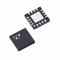
LT5517EUF Linear Technology, LT5517EUF Datasheet - Page 9

LT5517EUF
Manufacturer Part Number
LT5517EUF
Description
IC DEMOD QUAD 40-900MHZ 16-QFN
Manufacturer
Linear Technology
Datasheet
1.LT5517EUF.pdf
(12 pages)
Specifications of LT5517EUF
Function
Demodulator
Lo Frequency
80MHz ~ 1.8GHz
Rf Frequency
40MHz ~ 900MHz
P1db
10dBm
Gain
3.3dB
Noise Figure
12.4dB
Current - Supply
110mA
Voltage - Supply
4.5 V ~ 5.25 V
Package / Case
16-QFN
Lead Free Status / RoHS Status
Contains lead / RoHS non-compliant
Available stocks
Company
Part Number
Manufacturer
Quantity
Price
Company:
Part Number:
LT5517EUF
Manufacturer:
LT
Quantity:
10 000
Part Number:
LT5517EUF
Manufacturer:
LINEAR/凌特
Quantity:
20 000
Part Number:
LT5517EUF#PBF
Manufacturer:
LINEAR/凌特
Quantity:
20 000
Part Number:
LT5517EUF#TRPBF
Manufacturer:
LINEAR/凌特
Quantity:
20 000
APPLICATIO S I FOR ATIO
Table 2. RF Input Differential Impedance
2XLO Input Port
To ease the interface of the receiver with the external 2XLO
input, the 2XLO port is designed with on-chip 50 imped-
ance matching up to 2GHz. The input is internally biased
at 1V. A 1nF DC blocking capacitor is required when
connected to the external 2XLO source.
The 2XLO frequency is required to be twice the desired
operating frequency in order for the chip to generate the
FREQUENCY
(MHz)
100
200
300
400
500
600
700
800
900
40
DIFFERENTIAL INPUT
IMPEDANCE ( )
173.2-j105.8
156.2-j110.2
141.2-j111.8
129.5-j114.5
240.1-j10.3
245.5-j25.9
236.8-j50.0
223.6-j70.5
207.9-j86.3
190.6-j98.1
U
U
RF
Figure 6. RF Input Equivalent Circuit with External Broadband Matching
J1
W
0.665
0.664
0.664
0.663
0.662
0.660
0.657
0.655
0.651
0.650
MAG
DIFFERENTIAL S11
C10
3.3pF
5
4
U
ANGLE( )
MABAES0054
–10.2
–12.7
–15.3
–17.9
–20.4
–22.9
–0.8
–2.5
–5.1
–7.6
T1
1
2
3
1nF
1nF
C1
C2
quadrature Local Oscillator (LO) signals for the demodu-
lator. The on-chip divide-by-two circuit delivers well-
matched, quadrature LO carriers to the I mixer and the Q
mixer.
I-Channel and Q-Channel Outputs
Each of the I-channel and Q-channel outputs is internally
connected to V
bias voltage is V
or AC coupled to the external loads. The differential output
impedance of the demodulator is 120 in parallel with a
10pF internal capacitor, forming a lowpass filter with a
–3dB corner frequency at 130MHz. The load impedance,
R
gain is reduced by 20 • log(1 + 120 /R
the differential output is terminated by R
ample, the gain is reduced by 6.85dB when each output pin
is connected to a 50 load (or 100 differential loads).
The output should be taken differentially (or by using
differential-to-single-ended conversion) for best RF per-
formance, including NF and IM2. Proper filtering of the
unwanted high frequency mixing product is also impor-
tant to maintain the highest linearity. A convenient
LOAD
2
3
LT5517
RF
RF
, should be larger than 600 to assure full gain. The
+
–
V
CC
CC
CC
though a 60 resistor. The output DC
– 0.78V. The outputs can be DC coupled
250
2.30V
5517 F06
LOAD
LT5517
LOAD
) in dB when
. For ex-
9
5517f


