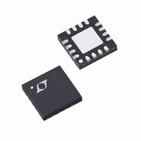
LT5517EUF Linear Technology, LT5517EUF Datasheet

LT5517EUF
Specifications of LT5517EUF
Available stocks
Related parts for LT5517EUF
LT5517EUF Summary of contents
Page 1
... Consequently, the outputs of the I-channel and the Q-channel are well matched in amplitude, and their phases are 90 apart. The LT5517 also provides excellent 50 impedance matching at the 2XLO port across its entire frequency range. , LTC and LT are registered trademarks of Linear Technology Corporation LT5517 CC ...
Page 2
... Consult LTC Marketing for parts specified with wider operating temperature ranges 5V CONDITIONS Internally Matched Source Voltage Gain, Load Impedance = 1k – 2-Tone, –10dBm/Tone 200kHz 2-Tone, –10dBm/Tone 200kHz (Note 4) (Note 4) Differential U W ORDER PART TOP VIEW NUMBER LT5517EUF GND 17 10 2XLO GND 9 UF PART MARKING UF PACKAGE 5517 = 37 C 799 ...
Page 3
DC ELECTRICAL CHARACTERISTICS PARAMETER Supply Voltage Supply Current Shutdown Current Turn-On Time Turn-Off Time EN = HIGH (On LOW (Off) EN Input Current Output DC Offset Voltage + – + – – – ...
Page 4
LT5517 W U TYPICAL PERFOR A CE CHARACTERISTICS f = 800MHz –10dBm, unless otherwise noted. (Test circuit shown in Figure 2) RF 2XLO I/Q Output Power, IM3 vs RF Input Power 1602MHz f = 799.9MHz ...
Page 5
W U TYPICAL PERFOR A CE CHARACTERISTICS f = 800MHz –10dBm, unless otherwise noted. (Test circuit shown in Figure 2) RF 2XLO RF-LO Isolation vs RF Input Power 120 110 f = 40MHz RF 100 ...
Page 6
LT5517 W BLOCK DIAGRA + RF 2 – I-MIXER 0 RF AMP LO BUFFERS 2 90 Q-MIXER BIAS GND ...
Page 7
TEST CIRCUIT R2 J1 MABAES0054 0 RF C10 3.3pF Figure 3. Component Side Silkscreen of Evaluation Board J3 – I OUT C15 C14 10pF 10pF OUT C16 C13 10pF 10pF 1nF ...
Page 8
LT5517 U U APPLICATIO S I FOR ATIO The LT5517 is a direct I/Q demodulator targeting high linearity receiver applications. It consists ampli- fier, I/Q mixers, a quadrature LO carrier generator and bias circuitry. The RF signal ...
Page 9
U U APPLICATIO S I FOR ATIO Table 2. RF Input Differential Impedance FREQUENCY DIFFERENTIAL INPUT (MHz) IMPEDANCE ( ) 40 240.1-j10.3 100 245.5-j25.9 200 236.8-j50.0 300 223.6-j70.5 400 207.9-j86.3 500 190.6-j98.1 600 173.2-j105.8 700 156.2-j110.2 800 141.2-j111.8 900 129.5-j114.5 ...
Page 10
LT5517 U U APPLICATIO S I FOR ATIO approach is to terminate each output with a shunt capaci- tor. The capacitor value can be optimized depending upon the operating frequency and the specific PCB layout. The phase relationship between the ...
Page 11
... MOLD FLASH. MOLD FLASH, IF PRESENT, SHALL NOT EXCEED 0.15mm ON ANY SIDE 4. EXPOSED PAD SHALL BE SOLDER PLATED Information furnished by Linear Technology Corporation is believed to be accurate and reliable. However, no responsibility is assumed for its use. Linear Technology Corporation makes no represen- tation that the interconnection of its circuits as described herein will not infringe on existing patent rights. U ...
Page 12
... Multiband GSM/DCS/GPRS Mobile Phones Multiband GSM/DCS/GPRS Phones, 45dB Dynamic Range, 450kHz Loop BW Multiband GSM/DCS/GPRS Phones, 45dB Dynamic Range, 250kHz Loop BW Multiband GSM/GPRS/EDGE Mobile Phones www.linear.com Offset Control, Adjustable Gain and Offset LT/TP 0104 1K • PRINTED IN USA LINEAR TECHNOLOGY CORPORATION 2004 5517f ...


