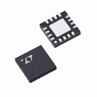
LT5506EUF Linear Technology, LT5506EUF Datasheet - Page 9

LT5506EUF
Manufacturer Part Number
LT5506EUF
Description
IC DEMOD QUADRATURE VGA 16QFN
Manufacturer
Linear Technology
Datasheet
1.LT5506EUF.pdf
(12 pages)
Specifications of LT5506EUF
Function
Demodulator
Lo Frequency
80MHz ~ 1GHz
Rf Frequency
40MHz ~ 500MHz
Gain
59dB
Noise Figure
6.8dB
Current - Supply
36mA
Voltage - Supply
1.8 V ~ 5.25 V
Package / Case
16-QFN
Lead Free Status / RoHS Status
Contains lead / RoHS non-compliant
P1db
-
Available stocks
Company
Part Number
Manufacturer
Quantity
Price
Part Number:
LT5506EUF
Manufacturer:
LINEAR/凌特
Quantity:
20 000
Company:
Part Number:
LT5506EUF#PBF
Manufacturer:
LT
Quantity:
3 360
Part Number:
LT5506EUF#PBF
Manufacturer:
LINEAR/凌特
Quantity:
20 000
Company:
Part Number:
LT5506EUF#TRPBF
Manufacturer:
ST
Quantity:
10 439
Part Number:
LT5506EUF#TRPBF
Manufacturer:
LINEAR/凌特
Quantity:
20 000
APPLICATIO S I FOR ATIO
voltage V
range is from V
nominal gain range from 0.9dB to 59dB. The linear-in-dB
gain relation with the V
voltages as low as –0.4 V. This results in an extended gain
control range of –19.7dB to 59dB. The V
sensitive input because of its high input impedance and
therefore should be well shielded. Signal pickup on the
V
I/Q baseband outputs. It can degrade the linearity perfor-
mance and it can cause asymmetry in the two-tone test. If
control speed is not important, 1 F bypass capacitors are
recommended between V
A fast responding peak detector is connected to the VGA
input, sensitive to signal levels above the signal levels
where the VGA is operating in the linear range. It is active
from –22dBm up to 5dBm IF input signal levels. The DC
output voltage of this detector (IF DET) can be used by the
baseband controller to quickly determine the presence of
a strong input level at the desired channel, and adjust gain
accordingly. Figure 3a shows the simplified circuit sche-
matic of the IF DET output.
I/Q Demodulators
The quadrature demodulators are double balanced mix-
ers, down-converting the amplified IF signal from the VGA
into I/Q baseband signals. The quadrature LO signals are
generated internally from a double frequency external CW
signal. The nominal output voltage of the differential I/Q
baseband signals should be set to 0.8V
depending on the linearity requirements. The magnitudes
of I and Q are well matched and their phases are 90 apart.
Quadrature LO Generator
The quadrature LO generator consists of a divide-by-two
circuit and LO buffers. An input signal (2xLO) with twice
the desired IF signal frequency is used as the clock for the
divide-by-two circuit, producing the quadrature LO signals
for the demodulators. The outputs are buffered and then
drive the down-converting mixers. With a fully differential
approach, the quadrature LO signals are well matched.
Second harmonic content (or higher order even harmon-
ics) in the external 2xLO signal can degrade the 90 phase
shift between I and Q. Therefore, such content should be
CTRL
pin can lead to spurs and increased noise floor in the
CTRL
can be set lower than 0.2V. The normal
CTRL
U
= 0.2V to 1.7V, which results in a
CTRL
CTRL
U
voltage still holds for control
and ground.
W
CTRL
P-P
pin is a very
U
or lower,
INPUT
minimized. Figure 3b shows the simplified circuit sche-
matic of the 2xLO inputs. Depending on the application,
different 2xLO input matching networks can be chosen. In
Figure 4, three examples are given. The first network pro-
vides the best 2xLO input sensitivity because it can boost
up the 2xLO differential input signal using a narrow-band
resonant approach. The second network gives a wide-band
match, but the 2xLO input sensitivity is about 2dB lower.
The third network gives a simple and less expensive wide-
band match, but 2xLO input sensitivity drops by about 9dB.
The IF input sensitivity doesn’t change significantly using
either of the three 2xLO matching networks.
Baseband Circuit
The baseband circuit consists of I/Q hard limiters (clip-
pers), I/Q lowpass filters and I/Q output buffers. The hard
limiter operates as a linear amplifier normally. However, if
a high level input temporarily overloads the linear ampli-
fier, then the circuit will limit symmetrically, which will
help to prevent the filter and output buffer from overload-
ing. This speeds up recovery from an overload event,
Figure 4. 2xLO Input Matching Networks for 4a) Narrow Band
Tuned to 570MHz, 4b) Wide Band, 4c) Single-Ended Wide Band
2xLO
V
3.3pF
(4a)
CC
3.8k
3.3pF
39nH
Figure 3a. Simplified Circuit Schematic of the
IF DET Output and Figure 3b. The 2xLO Inputs
(3a)
TO 2xLO
TO 2xLO
IF DET
–
+
INPUT
2xLO
2xLO
2xLO
V
CC
1:4
(4b)
+
–
240
TO 2xLO
TO 2xLO
1k
INPUT
8k
2xLO
–
+
(3b)
LT5506
56
100pF
(4c)
+
–
400mV
5506 F03
100pF
TO 2xLO
TO 2xLO
8k
5506 F04
5506fa
9
+
–


