MW6IC1940NBR1 Freescale Semiconductor, MW6IC1940NBR1 Datasheet - Page 2
MW6IC1940NBR1
Manufacturer Part Number
MW6IC1940NBR1
Description
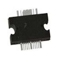
IC POWER AMP RF TO-272-16
Manufacturer
Freescale Semiconductor
Datasheet
1.MW6IC1940NBR1.pdf
(17 pages)
Specifications of MW6IC1940NBR1
Current - Supply
200mA
Frequency
1.92GHz ~ 2GHz
Gain
27dB
Package / Case
TO-272-16
Rf Type
Cellular, W-CDMA
Voltage - Supply
28V
Manufacturer's Type
Power Amplifier
Number Of Channels
1
Frequency (max)
2GHz
Operating Supply Voltage (min)
26V
Operating Supply Voltage (typ)
28V
Operating Supply Voltage (max)
32V
Package Type
TO-272 WB EP
Mounting
Surface Mount
Pin Count
16
Lead Free Status / RoHS Status
Contains lead / RoHS non-compliant
Noise Figure
-
P1db
-
Test Frequency
-
Lead Free Status / Rohs Status
Compliant
Available stocks
Company
Part Number
Manufacturer
Quantity
Price

Part Number:
MW6IC1940NBR1
Manufacturer:
FREESCALE
Quantity:
20 000


2
MW6IC1940GNBR1
Table 1. Maximum Ratings
Table 2. Thermal Characteristics
Table 3. ESD Protection Characteristics
Table 4. Moisture Sensitivity Level
Table 5. Electrical Characteristics
Functional Tests (In Freescale Wideband 1920--2000 MHz Test Fixture, 50 ohm system) V
P
3.84 MHz Channel Bandwidth @ ±10 MHz Offset. PAR = 8.5 dB @ 0.01% Probability on CCDF.
out
Drain--Source Voltage
Gate--Source Voltage
Storage Temperature Range
Case Operating Temperature
Operating Junction Temperature
Input Power
Thermal Resistance, Junction to Case
Human Body Model (per JESD22--A114)
Machine Model (per EIA/JESD22--A115)
Charge Device Model (per JESD22--C101)
Per JESD 22--A113, IPC/JEDEC J--STD--020
Power Gain
Power Added Efficiency
Intermodulation Distortion
Adjacent Channel Power Ratio
Input Return Loss
1. Continuous use at maximum temperature will affect MTTF.
2. MTTF calculator available at http://www.freescale.com/rf. Select Software & Tools/Development Tools/Calculators to access
3. Refer to AN1955, Thermal Measurement Methodology of RF Power Amplifiers. Go to http://www.freescale.com/rf.
W--CDMA Application
(P
= 4.5 W Avg., f1 = 1922.5 MHz, f2 = 1932.5 MHz, 2--Carrier W--CDMA, 3.84 MHz Channel Bandwidth @ ±5 MHz Offset. IM3 measured in
MTTF calculators by product.
Select Documentation/Application Notes -- AN1955.
out
= 4.5 W Avg.)
Test Methodology
Characteristic
Test Methodology
Characteristic
(1,2)
Rating
(T
A
Stage 2, 28 Vdc, I
Stage 1, 28 Vdc, I
= 25°C unless otherwise noted)
DQ1
DQ2
= 200 mA
= 440 mA
Symbol
Rating
ACPR
PAE
G
IM3
IRL
3
ps
Symbol
Symbol
DD
V
R
V
T
P
T
DSS
T
θJC
stg
GS
C
in
= 28 Vdc, I
J
12.5
Min
Package Peak Temperature
26
—
—
—
DQ1
1B (Minimum)
IV (Minimum)
A (Minimum)
28.5
13.5
260
Typ
--43
--46
--15
= 200 mA, I
--65 to +150
Value
Class
--0.5, +68
--0.5, +6
Value
150
225
2.1
1.2
20
Freescale Semiconductor
(2,3)
DQ2
Max
31.5
--40
--43
--10
—
= 440 mA,
RF Device Data
(continued)
°C/W
dBm
Unit
Unit
Vdc
Vdc
Unit
Unit
dBc
dBc
°C
°C
°C
dB
dB
°C
%
Related parts for MW6IC1940NBR1
Image
Part Number
Description
Manufacturer
Datasheet
Request
R

Part Number:
Description:
Manufacturer:
Freescale Semiconductor, Inc
Datasheet:
Part Number:
Description:
Manufacturer:
Freescale Semiconductor, Inc
Datasheet:
Part Number:
Description:
Manufacturer:
Freescale Semiconductor, Inc
Datasheet:
Part Number:
Description:
Manufacturer:
Freescale Semiconductor, Inc
Datasheet:
Part Number:
Description:
Manufacturer:
Freescale Semiconductor, Inc
Datasheet:
Part Number:
Description:
Manufacturer:
Freescale Semiconductor, Inc
Datasheet:
Part Number:
Description:
Manufacturer:
Freescale Semiconductor, Inc
Datasheet:
Part Number:
Description:
Manufacturer:
Freescale Semiconductor, Inc
Datasheet:
Part Number:
Description:
Manufacturer:
Freescale Semiconductor, Inc
Datasheet:
Part Number:
Description:
Manufacturer:
Freescale Semiconductor, Inc
Datasheet:
Part Number:
Description:
Manufacturer:
Freescale Semiconductor, Inc
Datasheet:
Part Number:
Description:
Manufacturer:
Freescale Semiconductor, Inc
Datasheet:
Part Number:
Description:
Manufacturer:
Freescale Semiconductor, Inc
Datasheet:
Part Number:
Description:
Manufacturer:
Freescale Semiconductor, Inc
Datasheet:
Part Number:
Description:
Manufacturer:
Freescale Semiconductor, Inc
Datasheet: