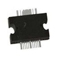
MW6IC1940NBR1 Freescale Semiconductor, MW6IC1940NBR1 Datasheet

MW6IC1940NBR1
Specifications of MW6IC1940NBR1
Available stocks
Related parts for MW6IC1940NBR1
MW6IC1940NBR1 Summary of contents
Page 1
... Refer to AN1977, Quiescent Current Thermal Tracking Circuit in the RF Integrated Circuit Family and to AN1987, Quiescent Current Control for the RF Integrated Circuit Device Family http://www.freescale.com/rf. Select Documentation/Application Notes -- AN1977 or AN1987. © Freescale Semiconductor, Inc., 2006--2009. All rights reserved. RF Device Data Freescale Semiconductor ...
Page 2
... Package Peak Temperature 260 Min Typ Max = 28 Vdc 200 mA 440 mA, DD DQ1 DQ2 26 28.5 31.5 12.5 13.5 — — --43 --40 — --46 --43 — --15 --10 (continued) RF Device Data Freescale Semiconductor Unit Vdc Vdc °C °C °C dBm Unit °C/W Unit °C Unit dB % dBc dBc dB ...
Page 3
... Duty Cycle) 1. Refer to AN1977, Quiescent Current Thermal Tracking Circuit in the RF Integrated Circuit Family and to AN1987, Quiescent Current Control for the RF Integrated Circuit Device Family http://www.freescale.com/rf. Select Documentation/Application Notes -- AN1977 or AN1987. RF Device Data Freescale Semiconductor (continued) = 25°C unless otherwise noted) A Symbol ...
Page 4
... Microstrip PCB Taconic TLX8--0300, 0.030″, ε * Variable for tuning Description C3225X5R1H225MT ATC100B0R5BT500XT ATC100B1R5BT500XT ATC100B0R2BT500XT ATC100B100JT500XT CRCW12064701FKEA CRCW12063301FKEA V D2 C10 C2 RF OUTPUT C11 C3 = 2.55 r Part Number Manufacturer TDK ATC ATC ATC ATC Vishay Vishay RF Device Data Freescale Semiconductor ...
Page 5
... V D1 MW6IC1940NB Rev Figure 4. MW6IC1940GNBR1 Test Circuit Component Layout RF Device Data Freescale Semiconductor C10 C11 MW6IC1940GNBR1 5 ...
Page 6
... Watts Avg. out --55 --60 --12 --14 --65 --16 --18 --70 --20 2000 = 26 dBm Avg. out 250 mA = 300 mA 150 mA 100 Vdc 440 mA DQ2 10 100 P , OUTPUT POWER (WATTS) PEP out Output Power @ I = 440 mA DQ2 RF Device Data Freescale Semiconductor 200 ...
Page 7
... Pulsed CW, 12 μsec(on), 1% Duty Cycle 1965 MHz INPUT POWER (dBm) in Figure 13. Pulsed CW Output Power versus Input Power RF Device Data Freescale Semiconductor TYPICAL CHARACTERISTICS --20 --25 --30 --35 --40 440 mA --45 -- 1955 MHz 1965 MHz Two--Tone Measurements, 10 MHz Tone Spacing --60 100 1 Figure 10. Third Order Intermodulation Distortion ...
Page 8
... JUNCTION TEMPERATURE (° Vdc 4.5 W Avg., and PAE = 13.5%. DD out I = 200 mA DQ1 I = 440 mA DQ2 f = 1960 MHz OUTPUT POWER (WATTS) CW out T = --30_C C 25_C 85_C = 4.5 W Avg. out = 440 mA DQ2 1840 1880 1920 1960 f, FREQUENCY (MHz) 230 250 RF Device Data Freescale Semiconductor 80 2000 ...
Page 9
... MHz f = 2040 MHz Figure 20. Series Equivalent Source and Load Impedance RF Device Data Freescale Semiconductor Ω load Vdc 200 mA 440 mA DQ1 DQ2 out f Z source MHz Ω 1880 69.33 + j26.65 3.65 -- j5.717 1900 65.20 + j19.39 3.55 -- j5.95 1920 61.07 + j12.13 3.45 -- j6.18 1940 56 ...
Page 10
... RF Device Data Freescale Semiconductor ...
Page 11
... RF Device Data Freescale Semiconductor ( 200 mA 440 mA DQ1 DQ2 ∠ φ 0.418 --141 0.003 0.367 --152 0.004 0.319 --162 0 ...
Page 12
... MW6IC1940GNBR1 12 PACKAGE DIMENSIONS RF Device Data Freescale Semiconductor ...
Page 13
... RF Device Data Freescale Semiconductor MW6IC1940GNBR1 13 ...
Page 14
... MW6IC1940GNBR1 14 RF Device Data Freescale Semiconductor ...
Page 15
... Corrected mm dimension L for gull--wing foot from 4.90--5.06 Min--Max to 0.46--0.61 Min--Max. Corrected L1 mm dimension from .025 BSC to 0.25 BSC. Added JEDEC Standard Package Number. • Data sheet archived. Part no longer manufactured. • Updated Product Documentation adding AN1907 and AN3263 Device Data Freescale Semiconductor PRODUCT DOCUMENTATION REVISION HISTORY Description 2 ...
Page 16
... Dec. 2009 • Corrected data sheet to reflect RF Test Reduction frequency described in Product and Process Change Notification number, PCN13232 • Rev. 3.1 (MW6IC1940GNBR1) data sheet archived. Part no longer manufactured. See Rev. 4.1 for MW6IC1940NBR1. MW6IC1940GNBR1 16 REVISION HISTORY (continued) Description RF Device Data ...
Page 17
... Freescale Semiconductor product could create a situation where personal injury or death may occur. Should Buyer ...


