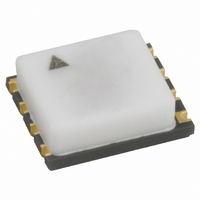
RF3800TR7 RFMD, RF3800TR7 Datasheet - Page 13

RF3800TR7
Manufacturer Part Number
RF3800TR7
Description
IC AMP HBT GAAS PRE-DVR 6W AIN
Manufacturer
RFMD
Datasheet
1.RF3800TR7.pdf
(18 pages)
Specifications of RF3800TR7
Current - Supply
400mA
Frequency
150MHz ~ 960MHz
Gain
14.7dB
Noise Figure
6.5dB
P1db
37dBm ~ 39.1dBm
Package / Case
8-LCC
Rf Type
W-CDMA, SATCOM
Test Frequency
450MHz
Voltage - Supply
5V ~ 8V
Lead Free Status / RoHS Status
Lead free / RoHS Compliant
Other names
689-1025-2
Note that I
evaluation board set up for 6 V linear operation at 20 dBm output power:
P
OIP3 = 47.5 dBm
Gain = 12 dB
OP1dB = 33.8 dBm
In comparison to 940 MHz data in application schematics section, we see lower gain and OP1dB. The reason for this delta is a
slightly different output match was used: 4.7 pF shunt output capacitor was changed to 5.6 pF for enhanced OIP3. This shows
the importance of output load impedance in each application. The application schematic match was intentionally set for high
OP1dB and efficiency, while the above case was geared for backed off linearity.
As mentioned above, one factor to keep in mind when increasing bias for low power linearity would be consideration of junction
temperature, T
approximate T
Dissipated power at 20 dBm = P
R
When matching RF3800 for a unique frequency not addressed in the data sheet, the following methodology has been proven
effective:
Rev A11 DS090624
OUT
TH
= 14.7°C/W. Thus, at 85 deg C ambient, T
= 20 dBm
4. As mentioned above, initial calculation was to determine starting point bias R. Refining by trial and error and using
standard R values yielded the following:
a. bias R = 20 Ω
b. V
c. I
d. I
e. V
1. Small signal s-parameters can be obtained from RFMD applications/sales. Using s2p data, matching topology/values
at input/output can be determined. This via simple Smith Chart matching, or simulation software.
2. Once acceptable small signal response is obtained, the match is evaluated for target specs:
a. Gain
b. Compression point
c. Linearity requirement
d. Efficiency and projected junction temperature at corresponding output power.
3. Output match optimization can now take place, such that specification compliance is achieved.
REF
CQ
CC
REF_PIN
REF
= 593 mA
= V
= 49 mA
J
REF
is just within limit of 50 mA called out in max ratings table on page 2. Measured data for this example, 940 MHz
J
at 85°C ambient for above 940 MHz, 20 dBm example:
. This becomes more critical as V
= 5.02 V
= 6 V
7628 Thorndike Road, Greensboro, NC 27409-9421 · For sales or technical
support, contact RFMD at (+1) 336-678-5570 or sales-support@rfmd.com.
DISS
= V
CC
* I
CC
- P
J
OUT
= 85 + 3.458 * 14.7 = 135.8°C.
CC
= 6 * 0.593 - 0.1 = 3.458 W. From data sheet R
is increased. As an exercise to demonstrate, use data sheet curves to
TH
versus P
RF3800
OUT
curve, we see
13 of 18


