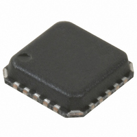
RF3866TR7 RFMD, RF3866TR7 Datasheet - Page 10

RF3866TR7
Manufacturer Part Number
RF3866TR7
Description
IC AMP LOW-NOISE 2-STAGE 20-QFN
Manufacturer
RFMD
Datasheet
1.RF3866TR7.pdf
(12 pages)
Specifications of RF3866TR7
Current - Supply
180mA ~ 220mA
Frequency
700MHz ~ 3.8GHz
Gain
20dB
Noise Figure
0.8dB
P1db
22dBm
Package / Case
20-QFN
Rf Type
Cellular, CDMA, PCS, DCS, UMTS, WLAN, 802.16/WiMax
Test Frequency
3.3GHz ~ 3.8GHz
Voltage - Supply
2.5V ~ 6V
Lead Free Status / RoHS Status
Lead free / RoHS Compliant
Available stocks
Company
Part Number
Manufacturer
Quantity
Price
Company:
Part Number:
RF3866TR7
Manufacturer:
RFMD
Quantity:
1 240
Part Number:
RF3866TR7
Manufacturer:
RFMD
Quantity:
20 000
RF3866
Low noise figure and high gain/IP3 make RF3866 ideal for use as both a receive LNA and a transmit driver for cellu-
lar/DCS/PCS/UMTS and WiMax platforms, in addition to many other general purpose applications. Standard evaluation boards
cover 700MHz to 1100MHz and 1800MHz to 3800MHz. Viewing the data sheet evaluation board schematic, refer below for
purpose and function of external components:
• R2/L4/C6 (0Ω/unpopulated/unpopulated on standard evaluation boards): These unused components were placed for
• L3/C5/C7: Place to optimize input match and enhance out of band low frequency stability.
• R3: Optionally placed to increase bias current and IP3. 20Ω value is found to be the best case (see graph section).
• L1/C3/R5/C8: Interstage tuning.
• L2/C4: Influence output return loss.
RF3866 has internal DC-blocking capacitors at RFin/RFout. In addition, it has been shown that impedance seen looking out at
pins 7/9/17/19 influence response. As a result, two port s-parameters become non-applicable. if matching is desired for fre-
quency bands outside of those provided with standard evaluation boards, application schematics within this data sheet for
400MHz to 1000MHz and 700MHz to 2200MHz serve as examples.
Detailed discussion of each begins here with the 400MHz to 1000MHz schematic. In this application the design goals were as
follows:
• Input and output return loss better than 10dB over the entire 600MHz bandwidth.
• IP3 and compression point in line with standard evaluation board performance.
These goals were attained, with additional specifications shown in tabular data accompanying schematic:
• Noise figure = 1.75dB to 1.25dB versus frequency
• Gain = 32.7dB to 30.8dB at band edges.
To extend the standard 700MHz to 1100MHz evaluation board response down to 400MHz, the following components were
changed (refer to reference designators in evaluation board schematic):
• C7 adjusted from unpopulated to 15pF
• L1 adjusted from 12nH to 27nH
• L2 adjusted from 8.2nH to 27nH
• “R5” adjusted from 6.8pF to 10pF
In effect, all components were placed or increased in value to shift response down in frequency. Broadband characteristic of
the part allowed return loss/performance to extend out to 1000MHz.
Next, consider the application schematic shown for 700MHz to 2200MHz. The design goals in this case:
• Maintain noise figure/IP3/OP1dB within reason to that seen on standard board.
• Obtain 2dB gain flatness over the 1500MHz bandwidth, along with better than 10dB input/output return loss.
10 of 12
convenience and flexibility when needed to optimize matching for an out of band application.
7628 Thorndike Road, Greensboro, NC 27409-9421 · For sales or technical
support, contact RFMD at (+1) 336-678-5570 or sales-support@rfmd.com.
Theory of Operation
DS100121


