WS2512-BLK Avago Technologies US Inc., WS2512-BLK Datasheet - Page 13
WS2512-BLK
Manufacturer Part Number
WS2512-BLK
Description
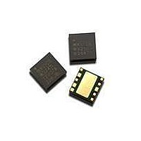
MODULE PA UMTS2100 4X4MM 10-PIN
Manufacturer
Avago Technologies US Inc.
Type
Power Amplifierr
Specifications of WS2512-BLK
Package / Case
10-DFN
Current - Supply
465mA ~ 510mA
Frequency
1.92GHz ~ 1.98GHz
Gain
23.5dB ~ 26.5dB
Rf Type
W-CDMA, HSPDA
Voltage - Supply
3.2V ~ 4.2V
Operating Frequency
1980 MHz
Operating Supply Voltage
4.2 V
Supply Current
510 mA
Maximum Operating Temperature
+ 90 C
Mounting Style
SMD/SMT
Minimum Operating Temperature
- 20 C
Number Of Channels
1 Channel
Frequency (max)
1.98GHz
Power Supply Requirement
Single
Single Supply Voltage (min)
3.2V
Single Supply Voltage (typ)
3.4V
Single Supply Voltage (max)
4.2V
Package Type
SMD
Dual Supply Voltage (min)
Not RequiredV
Dual Supply Voltage (typ)
Not RequiredV
Dual Supply Voltage (max)
Not RequiredV
Operating Temperature Classification
Commercial
Operating Temp Range
-20C to 90C
Pin Count
10
Mounting
Surface Mount
Lead Free Status / RoHS Status
Lead free / RoHS Compliant
Noise Figure
-
P1db
-
Test Frequency
-
Lead Free Status / Rohs Status
Compliant
Available stocks
Company
Part Number
Manufacturer
Quantity
Price

Part Number:
WS2512-BLK
Manufacturer:
AVAGO/安华高
Quantity:
20 000


13
PCB Design Guidelines
The recommended WS2512 PCB
Land pattern is shown in Figure
25 and Figure 26. The substrate
is coated with solder mask
between the I/O and conductive
paddle to protect the gold pads
from short circuit that is caused
by solder bleeding/bridging.
Stencil Design Guidelines
A properly designed solder
screen or stencil is required to
ensure optimum amount of
solder paste is deposited onto
the PCB pads.
The recommended stencil layout
is shown in Figure 27. Reducing
the stencil opening can poten-
tially generate more voids. On the
other hand, stencil openings
larger than 100% will lead to
excessive solder paste smear or
bridging across the I/O pads or
conductive paddle to adjacent
I/O pads. Considering the fact
that solder paste thickness will
directly affect the quality of the
solder joint, a good choice is to
use laser cut stencil composed of
0.100 mm (4mils) or 0.127 mm
(5mils) thick stainless steel
which is capable of
producing the required fine
stencil outline.
Figure 25. Metallization.
0.85
Figure 26. Solder Mask Opening.
Figure 27. Solder Paste Stencil Aperature.
0.85
0.85
0.5
0.4
0.4
0.25
0.7
0.8
0.7
2.0
0.1
1.6
0.8 x 0.5
0.8 x 0.6
on 0.6mm pitch
Ø 0.3mm
0.6
0.65
0.6
0.6
1.8
1.6
Related parts for WS2512-BLK
Image
Part Number
Description
Manufacturer
Datasheet
Request
R

Part Number:
Description:
MODULE PA UMTS2100 4X4MM 10-PIN
Manufacturer:
Avago Technologies US Inc.
Datasheet:

Part Number:
Description:
OPTOCOUPLER GATE DRV 2A 16-SOIC
Manufacturer:
Avago Technologies US Inc.
Datasheet:
Part Number:
Description:
OPTOCOUPLER 2CH 2.5A 16-SOIC
Manufacturer:
Avago Technologies US Inc.
Datasheet:

Part Number:
Description:
OPTOCOUPLER GATE DRV 0.4A 16SOIC
Manufacturer:
Avago Technologies US Inc.
Datasheet:

Part Number:
Description:
OPTOCOUPLER 2.0A 250KHZ 8-DIP
Manufacturer:
Avago Technologies US Inc.
Datasheet:

Part Number:
Description:
OPTOCOUPLER 2.0A 250KHZ GW 8-SMD
Manufacturer:
Avago Technologies US Inc.
Datasheet:

Part Number:
Description:
OPTOCOUPLER 2CH 15MBD 3.3V 8SOIC
Manufacturer:
Avago Technologies US Inc.
Datasheet:
Part Number:
Description:
OPTOCOUPLER DARL-OUT 8-DIP
Manufacturer:
Avago Technologies US Inc.
Datasheet:
Part Number:
Description:
OPTOCOUPLER IGBT DRIVE 0.4A 8DIP
Manufacturer:
Avago Technologies US Inc.
Datasheet:
Part Number:
Description:
OPTOCOUPLER DARL-OUT 8-DIP
Manufacturer:
Avago Technologies US Inc.
Datasheet:

Part Number:
Description:
OPTOCOUPLER 1CH 1MBS 8-SMD GW
Manufacturer:
Avago Technologies US Inc.
Datasheet:
Part Number:
Description:
OPTOCOUPLER GATE DRIVER 8-DIP
Manufacturer:
Avago Technologies US Inc.
Datasheet:

Part Number:
Description:
OPTOCOUPLER GATE DRIVER 8-SMD
Manufacturer:
Avago Technologies US Inc.
Datasheet:

Part Number:
Description:
OPTOCOUPLER PHOTOTRANS 4-SMD
Manufacturer:
Avago Technologies US Inc.
Datasheet:

Part Number:
Description:
OPTOCOUPLER W/BASE 6-DIP
Manufacturer:
Avago Technologies US Inc.
Datasheet: