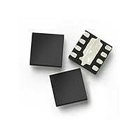
MGA-633P8-BLKG Avago Technologies US Inc., MGA-633P8-BLKG Datasheet
MGA-633P8-BLKG
Specifications of MGA-633P8-BLKG
MGA-633P8-BLKG
Available stocks


Related parts for MGA-633P8-BLKG


MGA-633P8-BLKG Summary of contents
Page 1
... It is designed for optimum use from 450MHz up to 2GHz. The compact footprint and low profile coupled with low noise, high gain and high linearity make the MGA-633P8 an ideal choice as a low noise amplifier for cellular infrastructure for GSM and CDMA. For optimum performance at higher frequency from 1.5GHz to 2.3GHz, the MGA-634P8 is recommended, and from 2 ...
Page 2
Absolute Maximum Rating T =25°C A Symbol Parameter V Device Voltage, RF output to ground dd I Drain Current Input Power max ( [3] P Total ...
Page 3
Product Consistency Distribution Charts LSL Id Max:67 Min:39 Mean: Figure 900MHz, 5V, 54mA Mean = 54 LSL OIP3 Min:34 Mean: ...
Page 4
... L1 C1 RFin Figure 6. Demo Board Schematic Diagram Note: x The schematic is shown with the assumption that similar PCB is used for all MGA-633P8, MGA-634P8 and MGA-635P8. x Detail of the components needed for this product is shown in Table 1. Value Detail Part Number 100pF (Murata) GRM1555C1H101JD01E 33nH (Toko) ...
Page 5
... MGA-633P8 Typical Performance RF performance 25°C, Vdd = 5V 54mA, measured using 50ohm input and output board, unless otherwise stated. A OIP3 test condition 900 MHz, F RF1 0.5 0.4 0.3 0.2 0 Idd (mA) Figure 7. Fmin vs Idd 700MHz Idd(mA) Figure 10. Gain vs Idd at 5V Tuned for Optimum OIP3 and Fmin at 700MHz ...
Page 6
Idd(mA) Figure 14. OP1dB vs Idd at 5V Tuned for Optimum OIP3 and Fmin at 700MHz 0.8 0.7 0.6 0.5 0.4 0.3 0.2 0.1 0 500 650 ...
Page 7
... Frequency (MHz) Figure 19. Fmin vs Frequency and Temperature for Optimum OIP3 and Fmin at 5V 54mA Below is the table showing the MGA-633P8 Reflection Coefficient Parameters tuned for Maximum OIP3, Vdd = 5V, Idd = 54mA. Gamma Load position Frequency (GHz) Magnitude 0.50 0.53 ...
Page 8
... MGA-633P8 Typical Performance in Demoboard RF performance 25°C, Vdd = 5V, Rbias = 6.8kOhm, measured on demo board in Figure.5 with component list in A Table1 for 900 MHz matching, unless otherwise stated. 0.8 0.7 0.6 0.5 0.4 0.3 0.2 -40°C 25°C 0.1 85° 500 1000 Frequency (MHz) Figure 22 Frequency vs Temperature ...
Page 9
... MGA-633P8 Typical Performance in Demoboard RF performance °C, Vdd =5V, Rbias=6.8kOhm, measured on demo board in Figure.5 with component list in A Table1 for 900 MHz matching, unless otherwise stated Rbias (Kohm) Figure 28. Idd vs Rbias 0.8 0.7 0.6 0.5 0.4 0.3 0.2 0 500 1000 Frequency (MHz) Figure 30 Frequency vs Idd ...
Page 10
... MGA-633P8 Typical Scattering Parameters, Vdd = 5V, Idd = 54mA S 11 Freq GHz Mag. Ang. 0.1 0.73 -45.42 0.5 0.25 -95.49 0.9 0.16 -119.26 1.0 0.15 -124.97 1.5 0.10 -142.55 1.9 0.07 -158.30 2.0 0.07 -162.64 2.5 0.05 177.70 3.0 0.03 162.14 4.0 0.01 -41 ...
Page 11
... PIN 1 DOT 2.00±0.050 BY MARKING 33X 2.00±0.050 Top View 0.60±0.050 Exp. DAP 0.35±0.050 0.25±0.050 Bottom View 11 Part Number Ordering Information * Part Number opt Ang. R MGA-633P8-BLKG n/50 -37 0.051 MGA-633P8-TR1G -17 0.0586 -15 0.0532 -13 0.0478 -7 0.0446 80.5 0.0644 98.7 0.0498 0.203 Ref. ...
Page 12
Recommended PCB Land Pattern and Stencil Design 2.20 1.75 0.00 0.80 0.50 0.25 0.45 0.30 R0.15 Land Pattern Combination of Land Pattern and Stencil Opening Note: 1. Recommended Land Pattern and Stencil Opening 2. Stencil thickness is 0.1mm (4 mils) ...
Page 13
Device Orientation REEL USER FEED COVER TAPE DIRECTION Tape Dimensions 10° Max A 0 DESCRIPTION CAVITY LENGTH WIDTH DEPTH PITCH BOTTOM HOLE DIAMETER PERFORATION DIAMETER PITCH POSITION CARRIER TAPE WIDTH THICKNESS COVER TAPE WIDTH TAPE ...
Page 14
Reel Dimensions – 7 inch 6.25mm EMBOSSED LETTERS LETTERING THICKNESS: 1.6mm SEE DETAIL "X" SLOT HOLE "b" SLOT HOLE(2x) 180° APART FRONT VIEW RECYCLE LOGO R10.65 R5.2 SLOT HOLE ‘b’ EMBOSSED RIBS RAISED: 0.25mm, WIDTH: 1.25mm ...