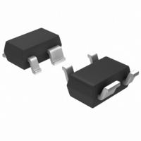
MGA-71543-BLKG Avago Technologies US Inc., MGA-71543-BLKG Datasheet - Page 5

MGA-71543-BLKG
Manufacturer Part Number
MGA-71543-BLKG
Description
IC AMP MMIC LNA GAAS 3V SOT-343
Manufacturer
Avago Technologies US Inc.
Type
General Purpose Amplifierr
Datasheet
1.MGA-71543-BLKG.pdf
(24 pages)
Specifications of MGA-71543-BLKG
P1db
13.1dBm
Noise Figure
1.1dB ~ 1.45dB
Package / Case
SC-70-4, SC-82-4, SOT-323-4, SOT-343
Current - Supply
50mA ~ 60mA
Frequency
100MHz ~ 6GHz
Gain
14.4dB ~ 17.4dB
Rf Type
CDMA, TDMA, W-CDMA
Test Frequency
2.01GHz
Voltage - Supply
2.7V ~ 4.2V
Mounting Style
SMD/SMT
Technology
Low Noise Amplifier
Number Of Channels
1
Operating Frequency
6000 MHz
Operating Supply Voltage
3 V
Supply Current
50 mA
Maximum Power Dissipation
200 mW
Maximum Operating Temperature
+ 150 C
Manufacturer's Type
Low Noise Amplifier
Frequency (max)
6GHz
Operating Supply Voltage (min)
2.7V
Operating Supply Voltage (typ)
3V
Operating Supply Voltage (max)
4.2V
Package Type
SOT-343
Mounting
Surface Mount
Pin Count
3 +Tab
Noise Figure (typ)
1.1@6000MHzdB
Lead Free Status / RoHS Status
Lead free / RoHS Compliant
Lead Free Status / RoHS Status
Lead free / RoHS Compliant, Lead free / RoHS Compliant
Other names
516-1952
MGA-71543-BLKG
MGA-71543-BLKG
Available stocks
Company
Part Number
Manufacturer
Quantity
Price
Company:
Part Number:
MGA-71543-BLKG
Manufacturer:
NXP
Quantity:
12 000
Part Number:
MGA-71543-BLKG
Manufacturer:
AVAGO/安华高
Quantity:
20 000
5
MGA-71543 Typical Performance, continued
T
and was optimized for each frequency with external tuners.
Notes:
4. P1dB measurements were performed with
Figure 15. Input Third Order Intercept Point
vs. Frequency and Current.
Figure 18. Minimum Noise Figure vs. Current
(2 GHz).
Figure 21. Control Voltage vs. Current.
c
passive biasing in Production Test Circuit
(Figure 4.). Quiescent drain current, Idsq, is
set by a fixed Vref with no RF drive applied.
As P1dB is approached, the drain current may
increase or decrease depending on frequency
and DC bias point which typically results in
2.2
2.0
1.8
1.6
1.4
1.2
1.0
0.8
0.6
0.4
0.2
1.0
0.8
0.6
0.4
0.2
= 25°C, Z
18
15
12
-3
9
6
3
0
0
0
0
0
0
1
o
10
10
= 50, V
FREQUENCY (GHz)
I
I
2
d
d
CURRENT (mA)
CURRENT (mA)
20
20
3
d
= 3V, I
4
30
30
d
= 10 mA unless stated otherwise. Data vs. frequency was measured in Figure 5 test system
5
6 mA
10 mA
20 mA
40
40
6
5. P1dB measurements were performed in
Figure 16. Output Power at 1 dB Compression
vs. I
Bias, V
Figure 19. Gain vs. Current and Temperature
(2 GHz).
higher P1dB than if the drain current is
maintained constant by active biasing.
Evaluation Test Circuit with source resistor
biasing which maintains the drain current
near the quiescent value under large signal
conditions.
18
15
12
20
17
14
11
-6
-3
9
3
0
8
5
2
dsq
0
0
ref
Current and Temperature (Passive
Fixed)
10
10
I
dsq
I
[4]
d
CURRENT (mA)
.
CURRENT (mA)
20
20
30
30
-40°C
+25°C
+85°C
-40°C
+25°C
+85°C
40
40
Figure 17. Output Power at 1 dB Compression
vs. Current and Temperature (Source Resistor
Bias in Evaluation Circuit)
Figure 20. Input Third Intercept Point vs.
Current and Temperature (2 GHz).
18
15
12
12
-3
-3
9
6
3
0
9
6
3
0
0
0
10
10
I
I
d
d
CURRENT (mA)
CURRENT (mA)
20
20
[5]
.
30
30
-40°C
+25°C
+85°C
-40°C
+25°C
+85°C
40
40


