MGA-71543-BLKG Avago Technologies US Inc., MGA-71543-BLKG Datasheet
MGA-71543-BLKG
Specifications of MGA-71543-BLKG
MGA-71543-BLKG
Available stocks


Related parts for MGA-71543-BLKG


MGA-71543-BLKG Summary of contents
Page 1
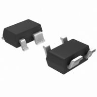
... LNA mode, 80% bypass. With the bypass current draw of zero and LNA of 10 mA, the MGA-71543 allows an average 2 mA current. The MGA-71543 is a GaAs MMIC, processed on Avago’s cost effec- tive PHEMT (Pseudomorphic High Electron Mobility Transistor Technology housed in the SOT343 (SC70 4-lead) package. ...
Page 2
... Functional Block Diagram OUT Switch & Bias MGA-71543 Absolute Maximum Ratings Symbol Parameter V Maximum Input to Output Voltage d V Maximum Input to Ground DC Voltage c I Supply Current d [2] P Power Dissipation Input Power in T Junction Temperature j T Storage Temperature STG Product Consistency Distribution Charts 150 Cpk = 2 ...
Page 3
... MGA-71543 Electrical Specifications T = +25° 50Ω mA 3V, unless noted Symbol Parameter and Test Condition Vref test Vds = 2 test f = 2.01 GHz Vds - Vref) d Gain test f = 2.01 GHz Vds - Vref) d IIP3 test f = 2.01 GHz Vds - Vref) d Gain, Bypass f = 2.01 GHz ...
Page 4
... Figure 9. Associated Gain with Fmin vs. Frequency 500 MHz to 6 GHz Figure 12. S22 Impedance vs. Frequency. ( Input Bias Tee ref RF Output 56 pF Figure 5. MGA-71543 Test Circuit for S, Noise, and Power Parameters over Frequency 2.7V 3.0V 3. FREQUENCY (GHz) Figure 7. Associated Gain with Fmin vs. ...
Page 5
... MGA-71543 Typical Performance, continued T = 25° unless stated otherwise. Data vs. frequency was measured in Figure 5 test system and was optimized for each frequency with external tuners FREQUENCY (GHz) Figure 15. Input Third Order Intercept Point vs. Frequency and Current. 2.2 2.0 1.8 1.6 1 ...
Page 6
... MGA-71543 Typical Scattering Parameters T = 25° 0V -3.0V (bypass mode ref d Freq (GHz) Mag. Ang. Mag. Ang. 0.1 0.968 -4.5 0.021 41.1 0.2 0.961 -8.4 0.039 70.5 0.3 0.951 -11.4 0.065 73.7 0.4 0.947 -14.8 0.09 70.9 0.5 0.937 -18.1 0.114 65.7 ...
Page 7
... MGA-71543 Typical Scattering Parameters and Noise Parameters T = 25° 2. -0. ref Freq (GHz) Mag. Ang. Mag. 0.3 0.927 -10.1 2.945 0.5 0.921 -16.4 2.939 0.7 0.915 -22.7 2.907 0.9 0.909 -28.8 2.871 1.1 0.899 -34.8 2.826 1.3 0.891 -40.5 2.783 1.5 ...
Page 8
... MGA-71543 Typical Scattering Parameters and Noise Parameters T = 25° ref d Freq (GHz) Mag. Ang. Mag. Ang. 0.3 0.911 -11 4.164 170.2 0.5 0.904 -17.7 4.148 163.3 0.7 0.896 -24.5 4.094 157.1 0.9 0.887 -31.2 4.029 151.1 1.1 0.875 -37.5 3.953 145.2 1 ...
Page 9
... MGA-71543 Typical Scattering Parameters and Noise Parameters T = 25° ref d Freq (GHz) Mag. Ang. Mag. Ang. 0.3 0.9 -11.5 5.023 169.8 0.5 0.892 -18.6 4.993 162.7 0.7 0.884 -25.7 4.919 156.3 0.9 0.873 -32.7 4.83 150 1.1 0.859 -39.4 4.728 143 ...
Page 10
... MGA-71543 Typical Scattering Parameters and Noise Parameters T = 25° ref d Freq (GHz) Mag. Ang. Mag. Ang. 0.3 0.889 -12.1 5.952 169.3 0.5 0.88 -19.5 5.901 162 0.7 0.87 -27 5.803 155.3 0.9 0.858 -34.3 5.684 148.8 1.1 0.842 -41.2 5.548 142.5 1 ...
Page 11
... MGA-71543 Typical Scattering Parameters and Noise Parameters T = 25° ref d Freq (GHz) Mag. Ang. Mag. 0.3 0.889 -12.3 6.174 0.5 0.88 -19.8 6.117 0.7 0.87 -27.4 6.012 0.9 0.857 -34.9 5.885 1.1 0.841 -41.9 5.74 1.3 0.823 -48.7 5.589 1.5 ...
Page 12
... Part Number Devices MGA-71543-TR1 3000 MGA-71543-TR2 10000 MGA-71543-BLK 100 MGA-71543-TR1G 3000 MGA-71543-TR2G 10000 MGA-71543-BLKG 100 Note: For lead-free option, the part number will have the character “G” at the end. Package Dimensions Outline 43 SOT-343 (SC70 4-lead) 1.30 (.051) BSC HE 1.15 (.045) BSC b1 ...
Page 13
Device Orientation REEL CARRIER TAPE USER FEED DIRECTION COVER TAPE Tape Dimensions For Outline DESCRIPTION CAVITY LENGTH WIDTH DEPTH PITCH BOTTOM HOLE DIAMETER PERFORATION DIAMETER PITCH POSITION CARRIER TAPE WIDTH THICKNESS COVER TAPE WIDTH TAPE ...
Page 14
... LNA and 80% bypass mode. For example, with the bypass draw of zero and LNA of 10 mA, the MGA-71543 allows an average of only 2 mA current. The MGA-71543 is a GaAs MMIC, processed on Avago’s cost effec- tive PHEMT (Pseudomorphic High Electron Mobility Transistor Technology housed in the SOT343 (SC70 4-lead) package ...
Page 15
... For applications in which input power levels vary over a wide range, it may be useful to dynami- cally adapt the bias of the MGA-71543 to match the signal level. A sensor senses the signal level at some point in the system (usually in the baseband circuitry) and automatically adjusts the bias current of the amplifier accord- ingly ...
Page 16
... If a lower current is drawn, the gain of the amplifier is significantly reduced and the performance will degrade. If the device current is set to zero, the MGA-71543 is switched into a bypass mode in which the signal is routed around the amplifier with a loss of about 5.6 dB. The simplest way of switching the ...
Page 17
... For low noise amplifier application, the LNA is typically biased mA. The MGA-71543 is a conditionally stable device, therefore, the proper input and output loads must be presented in addition to properly RF grounding the device. Please refer to the stability section for tips on preventing oscillation ...
Page 18
... Design for Stability The main potential for oscillation with the MGA-71543 is improper grounding and/or improper RF bypass capacitors. Any device with gain can be made to oscillate if feedback is added. Proper grounding may be achieved by minimizing inductance paths to the ground plane ...
Page 19
... To assist designers in optimizing not only the immediate amplifier circuit using the MGA-71543, but to also evaluate and optimize tradeoffs that affect a complete wireless system, the standard deviation (σ) is provided for many of the Electrical Specifica- tion parameters (at 25° ...
Page 20
Demonstration Board Source unstable G = 18.8 dB Load unstable region 16.8 dB Load stable region ...
Page 21
... OUT REV 2 Part Number 800 MHz [1] DUT MGA-71543 8.2 pF 100 pF 2.7 pF 0.01 µ TOKO LL1005 33 nH TOKO LL1005 33 nH TOKO LL1005 51Ω 115Ω — / LL1608-FH or 1005-FH 60Ω Package SOT-343 (4 lead SC-70 package) Size 0402 Size 0402 Size 0402 Size 0603 or 0402 ...
Page 22
... MGA-71543 Figure 24. System Level Overview of MGA-71543 for Handset Designers. These are the actual necessary components. The other connectors and board space are only for production. blue2_lna rev2.1 L25 C12 C36 R37 C38 U2 C47 L7 C44 C9 R38 R25 C37 R24 33.1 mm R21 C8 1.303 in ...
Page 23
... Not used Note 1: Device under Test Table 2. Component Values for 1900 MHz Amplifier on Smaller Board. References 1. Application note RLM020199, “Designing with the MGA-72543 RFIC Amplifier/Bypass Switch”. 2. G.D.Vendelin, A.M.Pavio and U.L.Rhode, “Microwave Circuit Design Using Linear and Nonlinear Techniques”. 23 Part Number ...
Page 24
... R38 R25 C37 R24 R21 C8 R20 C36 R38 C12 L5 C47 C37 C44 R25 R24 R21 R16 (0Ω Jumper) FDG6303N Selects current set by R21 Selects current set by R20 MGA-71543 RF OUT Switch & Bias Control SC70 FDG6303N Dual N-channel, Digital FET OUT Volt ...