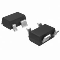
MGA-53543-TR1G Avago Technologies US Inc., MGA-53543-TR1G Datasheet - Page 9

MGA-53543-TR1G
Manufacturer Part Number
MGA-53543-TR1G
Description
IC AMP RFIC 1.9GHZ SOT-343
Manufacturer
Avago Technologies US Inc.
Datasheet
1.MGA-53543-TR1G.pdf
(14 pages)
Specifications of MGA-53543-TR1G
Gain
14dB ~ 17dB
Rf Type
Cellular, PCS
Current - Supply
40mA ~ 70mA
Frequency
0Hz ~ 2.4GHz
Noise Figure
1.5dB ~ 1.9dB
P1db
18.6dBm
Package / Case
SC-70-4, SC-82-4, SOT-323-4, SOT-343
Test Frequency
1.9GHz
Voltage - Supply
5V ~ 5.5V
Frequency Range
50MHz To 6GHz
Noise Figure Typ
1.5dB
Power Dissipation Pd
400mW
Supply Current
54mA
Supply Voltage Range
5V
Manufacturer's Type
Linear Amplifier
Number Of Channels
1
Frequency (max)
6GHz
Operating Supply Voltage (max)
5.5V
Package Type
SOT-343
Mounting
Surface Mount
Pin Count
3 +Tab
Noise Figure (typ)
1.9@2400MHzdB
Lead Free Status / RoHS Status
Lead free / RoHS Compliant
Lead Free Status / RoHS Status
Lead free / RoHS Compliant, Lead free / RoHS Compliant
Other names
516-1826-2
MGA-53543-TR1G
MGA-53543-TR1G
Available stocks
Company
Part Number
Manufacturer
Quantity
Price
Company:
Part Number:
MGA-53543-TR1G
Manufacturer:
AVAGO
Quantity:
15 600
Company:
Part Number:
MGA-53543-TR1G
Manufacturer:
AVAGO
Quantity:
11 800
Part Number:
MGA-53543-TR1G
Manufacturer:
AVAGO/安华高
Quantity:
20 000
To accomplish the above performance, a high pass con-
figuration consisting of a 3.3 nH inductor and a . pF
capacitor is used for the input match. Unlike a low pass
configuration, a high pass configuration provides not
only the impedance transfer required, but also provides
excellent stability for the demo board by diminishing low
frequency gain.
No matching is required for the output, but a good rule
of thumb to use when biasing is to limit series reactance
to less than 5Ω and keep shunt reactance above 500Ω.
Therefore choosing an RFC of 47 nH, which has a reac-
tance of 561Ω at 1.9 GHz, helps isolate the DC supply from
inband signals. If any high frequency signal is created or
enters the DC supply, a 150 pF capacitor is ready to short
it to ground. An 8. pF capacitor serves primarily as a DC
block, but also helps the output match.
The completed 1900 MHz amplifier schematic is shown
in Figure 19.
RF
Figure 19. Schematic for a 1900 MHz stable circuit.
Included with the schematic is a complete RF layout (Fig-
ure 4) which includes placement of all components and
SMA connectors. A list of part numbers and manufacturer
used is given below in Table 3.
Table 3. Component parts list for the MGA-53543 HLA at 1900 MHz.
3.3 nH
47 nH
.Ω
. pF
8. pF
150 pF
0.1 µF
Performance of MGA-53543 at 1900 MHz
With a device voltage of +5V, demonstration board MGA-
5X delivers a measured noise figure of 1.78 dB and an
average gain of 14.5 dB as shown in Figure 0. Gain here
is slightly lower than data sheet due to the losses acquired
in creating a stable broadband match. Input and output
VSWR are both better than :1 at 1900 MHz, with input
return loss being 10 dB and output return loss at 13 dB.
9
in
3.3 nH
TOKO LL1608-FS3N3S
TOKO LL1005-FH47N
RHOM MCR01JR
Phycomp 040CG9C9B00
Phycomp 040CG89D9B00
Phycomp 040CG151J9B00
Phycomp 0603F104M8B0
2.2 pF
1
3
53
2
4
+5V
2.2Ω
47 nH
8.2 pF
0.1 µF
150 pF
RF
out
Figure 20. Gain and Noise Figure vs Frequency.
Figure 21. Input and Output return loss vs Frequency.
More significant is the linearity delivered by MGA-53543
at 1900 MHz. Figure plots OIP3 over a frequency range
from 1850 MHz to1950 MHz.
This device produces IIP3 of 4 dBm, OIP3 of 38 dBm and
P1dB of 17.8 dBm at 1900 MHz.
Figure 22. OIP3 vs. Frequency.
Due to component parasitics and part variations, actual
performance may not be identical to this example.
Figure 11. Gain and Noise Figure vs
Frequency.
Figure 12. Input and Output Return Loss vs
Frequency.
Figure 13. OIP3 vs Frequency.
-10
-15
-20
-25
20
15
10
45
40
35
30
25
-5
5
0
0
1840
1.6
1.6
1.8
1.8
TX
1880
FREQUENCY (MHz)
FREQUENCY (GHz)
FREQUENCY (GHz)
2
2
1920
2.2
2.2
S11
S22
Gain
1960
RX
NF
2.4
2.4
2000
2.6
2.6


