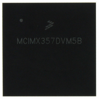
MCIMX357DVM5B Freescale Semiconductor, MCIMX357DVM5B Datasheet - Page 104

MCIMX357DVM5B
Manufacturer Part Number
MCIMX357DVM5B
Description
PROCESSOR MULTIMEDIA 400PBGA
Manufacturer
Freescale Semiconductor
Series
i.MX35r
Datasheet
1.MCIMX35WPDKJ.pdf
(148 pages)
Specifications of MCIMX357DVM5B
Core Processor
ARM11
Core Size
32-Bit
Speed
532MHz
Connectivity
1-Wire, CAN, EBI/EMI, Ethernet, I²C, MMC, SPI, SSI, UART/USART, USB OTG
Peripherals
DMA, I²S, LCD, POR, PWM, WDT
Number Of I /o
96
Program Memory Type
ROMless
Ram Size
128K x 8
Voltage - Supply (vcc/vdd)
1.33 V ~ 1.47 V
Oscillator Type
External
Operating Temperature
-20°C ~ 70°C
Package / Case
400-BGA
Operating Temperature (min)
-20C
Operating Temperature (max)
70C
Operating Temperature Classification
Commercial
Mounting
Surface Mount
Embedded Interface Type
CAN, I2C, SPI, UART, USB
Digital Ic Case Style
BGA
No. Of Pins
400
Operating Temperature Range
-20°C To +70°C
Processor Type
I.MX35
Lead Free Status / RoHS Status
Lead free / RoHS Compliant
Eeprom Size
-
Program Memory Size
-
Data Converters
-
Lead Free Status / Rohs Status
Compliant
Available stocks
Company
Part Number
Manufacturer
Quantity
Price
Company:
Part Number:
MCIMX357DVM5B
Manufacturer:
Freescale Semiconductor
Quantity:
10 000
Part Number:
MCIMX357DVM5B
Manufacturer:
FREESCALE
Quantity:
20 000
Company:
Part Number:
MCIMX357DVM5BR2
Manufacturer:
Freescale Semiconductor
Quantity:
10 000
Figure 78
timing parameters for MDMA read and write.
104
Parameter
tg(write)
tg(read)
tf(write)
tf(read)
tm, ti
ATA
td
t0
tL
tk
shows timing for MDMA read, and
Parameter
Figure
Figure 79
td, td1
i.MX35 Applications Processors for Industrial and Consumer Products, Rev. 9
from
tgr
tm
—
tfr
—
—
—
tk
78,
Table 68. MDMA Read and Write Timing Parameters
tm (min.) = ti (min.) = time_m × T – (tskew1 + tskew2 + tskew5)
td1.(min.) = td (min.) = time_d × T – (tskew1 + tskew2 + tskew6)
tk.(min.) = time_k × T – (tskew1 + tskew2 + tskew6)
t0 (min.) = (time_d + time_k) × T
tgr (min. – read) = tco + tsu + tbuf + tbuf + tcable1 + tcable2
tgr.(min. – drive) = td – te(drive)
tfr (min. – drive) = 0
tg (min. – write) = time_d × T – (tskew1 + tskew2 + tskew5)
tf (min. – write) = time_k × T – (tskew1 + tskew2 + tskew6)
tL (max.) = (time_d + time_k–2) × T – (tsu + tco + 2 × tbuf + 2 × tcable2)
Figure 78. MDMA Read Timing Diagram
Figure 79. MDMA Write Timing Diagram
Figure 79
shows timing for MDMA write.
Value
Freescale Semiconductor
Table 68
time_d, time_k
time_d, time_k
Controlling
Variable
time_m
time_d
time_d
time_d
time_k
time_k
lists the
—


