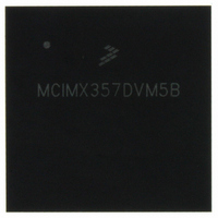
MCIMX357DVM5B Freescale Semiconductor, MCIMX357DVM5B Datasheet - Page 100

MCIMX357DVM5B
Manufacturer Part Number
MCIMX357DVM5B
Description
PROCESSOR MULTIMEDIA 400PBGA
Manufacturer
Freescale Semiconductor
Series
i.MX35r
Datasheet
1.MCIMX35WPDKJ.pdf
(148 pages)
Specifications of MCIMX357DVM5B
Core Processor
ARM11
Core Size
32-Bit
Speed
532MHz
Connectivity
1-Wire, CAN, EBI/EMI, Ethernet, I²C, MMC, SPI, SSI, UART/USART, USB OTG
Peripherals
DMA, I²S, LCD, POR, PWM, WDT
Number Of I /o
96
Program Memory Type
ROMless
Ram Size
128K x 8
Voltage - Supply (vcc/vdd)
1.33 V ~ 1.47 V
Oscillator Type
External
Operating Temperature
-20°C ~ 70°C
Package / Case
400-BGA
Operating Temperature (min)
-20C
Operating Temperature (max)
70C
Operating Temperature Classification
Commercial
Mounting
Surface Mount
Embedded Interface Type
CAN, I2C, SPI, UART, USB
Digital Ic Case Style
BGA
No. Of Pins
400
Operating Temperature Range
-20°C To +70°C
Processor Type
I.MX35
Lead Free Status / RoHS Status
Lead free / RoHS Compliant
Eeprom Size
-
Program Memory Size
-
Data Converters
-
Lead Free Status / Rohs Status
Compliant
Available stocks
Company
Part Number
Manufacturer
Quantity
Price
Company:
Part Number:
MCIMX357DVM5B
Manufacturer:
Freescale Semiconductor
Quantity:
10 000
Part Number:
MCIMX357DVM5B
Manufacturer:
FREESCALE
Quantity:
20 000
Company:
Part Number:
MCIMX357DVM5BR2
Manufacturer:
Freescale Semiconductor
Quantity:
10 000
1
4.9.17
The parallel ATA module can work on PIO/multiword DMA/ultra-DMA transfer modes (not available for
the MCIMX351). Each transfer mode has a different data transfer rate, Ultra DMA mode 4 data transfer
rate is up to 100 MBps.
The parallel ATA module interface consists of a total of 29 pins. Some pins have different functions in
different transfer modes. There are various requirements for timing relationships among the function pins,
in compliance with the ATA/ATAPI-6 specification, and these requirements are configurable by the ATA
module registers.
4.9.17.1
Table 64
4.9.17.2
This section discusses ATA parameters. For a detailed description, refer to the ATA-6 specification.
Level shifters are required for 3.3-V or 5.0-V compatibility on the ATA interface.
The use of bus buffers introduces delays on the bus and introduces skew between signal lines. These
factors make it difficult to operate the bus at the highest speed (UDMA-5) when bus buffers are used. Use
of bus buffers is not recommended if fast UDMA mode is required.
The ATA specification imposes a slew rate limit on the ATA bus. According to this limit, any signal driven
on the bus should have a slew rate between 0.4 and 1.2 V/ns with a 40 pF load. Few vendors of bus buffers
specify the slew rate of the outgoing signals.
When bus buffers are used the ata_data bus buffer is bidirectional, and uses the direction control signal
ata_buffer_en. When ata_buffer_en is asserted, the bus should drive from host to device. When
100
SI1
SI2
SI3
ID
SRISE and SFALL meet this requirement when measured at the sender’s connector from 10–90% of full signal amplitude with
all capacitive loads from 15 pF through 40 pF, where all signals have the same capacitive load value.
ATA Interface Signals
Rising edge slew rate for any signal on the ATA interface
Falling edge slew rate for any signal on the ATA interface
Host interface signal capacitance at the host connector
and
Parallel ATA Module AC Electrical Specifications
General Timing Requirements
Figure 75
ATA Electrical Specifications (ATA Bus, Bus Buffers)
i.MX35 Applications Processors for Industrial and Consumer Products, Rev. 9
define the AC characteristics of the interface signals on all data transfer modes.
Table 64. AC Characteristics of All Interface Signals
Figure 75. ATA Interface Signals Timing Diagram
Parameter
SI2
1
1
SI1
Symbol
S
C
S
rise
fall
host
1
1
Freescale Semiconductor
Min.
—
—
—
Max.
1.25
1.25
20
Unit
V/ns
V/ns
pF


