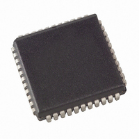
ATMEGA8515L-8JU Atmel, ATMEGA8515L-8JU Datasheet - Page 66

ATMEGA8515L-8JU
Manufacturer Part Number
ATMEGA8515L-8JU
Description
MCU AVR 8K ISP FLASH MEM 44-PLCC
Manufacturer
Atmel
Series
AVR® ATmegar
Specifications of ATMEGA8515L-8JU
Core Processor
AVR
Core Size
8-Bit
Speed
8MHz
Connectivity
EBI/EMI, SPI, UART/USART
Peripherals
Brown-out Detect/Reset, POR, PWM, WDT
Number Of I /o
35
Program Memory Size
8KB (4K x 16)
Program Memory Type
FLASH
Eeprom Size
512 x 8
Ram Size
512 x 8
Voltage - Supply (vcc/vdd)
2.7 V ~ 5.5 V
Oscillator Type
Internal
Operating Temperature
-40°C ~ 85°C
Package / Case
44-LCC (J-Lead)
Processor Series
ATMEGA8x
Core
AVR8
Data Bus Width
8 bit
Data Ram Size
512 B
Interface Type
SPI, USART
Maximum Clock Frequency
8 MHz
Number Of Programmable I/os
35
Number Of Timers
2
Operating Supply Voltage
2.7 V to 5.5 V
Maximum Operating Temperature
+ 85 C
Mounting Style
SMD/SMT
3rd Party Development Tools
EWAVR, EWAVR-BL
Minimum Operating Temperature
- 40 C
Cpu Family
ATmega
Device Core
AVR
Device Core Size
8b
Frequency (max)
8MHz
Total Internal Ram Size
512Byte
# I/os (max)
35
Number Of Timers - General Purpose
2
Operating Supply Voltage (typ)
3.3/5V
Operating Supply Voltage (max)
5.5V
Operating Supply Voltage (min)
2.7V
Instruction Set Architecture
RISC
Operating Temp Range
-40C to 85C
Operating Temperature Classification
Industrial
Mounting
Surface Mount
Pin Count
44
Package Type
PLCC
For Use With
ATSTK600 - DEV KIT FOR AVR/AVR32770-1007 - ISP 4PORT ATMEL AVR MCU SPI/JTAGATAVRISP2 - PROGRAMMER AVR IN SYSTEMATSTK500 - PROGRAMMER AVR STARTER KIT
Lead Free Status / RoHS Status
Lead free / RoHS Compliant
Data Converters
-
Lead Free Status / Rohs Status
Details
Available stocks
Company
Part Number
Manufacturer
Quantity
Price
Part Number:
ATMEGA8515L-8JU
Manufacturer:
ATMEL/爱特梅尔
Quantity:
20 000
Special Function IO Register –
SFIOR
Alternate Functions of Port A
66
ATmega8515(L)
• Bit 2 – PUD: Pull-up Disable
When this bit is written to one, the pull-ups in the I/O ports are disabled even if the DDxn
and PORTxn Registers are configured to enable the pull-ups ({DDxn, PORTxn} = 0b01).
See “Configuring the Pin” on page 60 for more details about this feature.
Port A has an alternate function as the address low byte and data lines for the External
Memory Interface.
Table 26. Port A Pins Alternate Functions
Table 27 and Table 28 relate the alternate functions of Port A to the overriding signals
shown in Figure 33 on page 64.
Table 27. Overriding Signals for Alternate Functions in PA7..PA4
Note:
Bit
Read/Write
Initial Value
Signal
Name
PUOE
PUOV
DDOE
DDOV
PVOE
PVOV
DIEOE
DIEOV
DI
AIO
Port Pin
PA7
PA6
PA5
PA4
PA3
PA2
PA1
PA0
1. ADA is short for ADdress Active and represents the time when address is output. See
“External Memory Interface” on page 25.
PA7/AD7
SRE
~(WR | ADA
PortA7
SRE
WR | ADA
SRE
A7 • ADA |
D7 OUTPUT • WR
0
0
D7 INPUT
–
R/W
7
–
0
Alternate Function
AD7 (External memory interface address and data bit 7)
AD6 (External memory interface address and data bit 6)
AD5 (External memory interface address and data bit 5)
AD4 (External memory interface address and data bit 4)
AD3 (External memory interface address and data bit 3)
AD2 (External memory interface address and data bit 2)
AD1 (External memory interface address and data bit 1)
AD0 (External memory interface address and data bit 0)
XMBK
R/W
(1)
6
0
) •
XMM2
R/W
PA6/AD6
SRE
~(WR | ADA) •
PortA6
SRE
WR | ADA
SRE
A6 • ADA |
D6 OUTPUT •
WR
0
0
D6 INPUT
–
5
0
XMM1
R/W
4
0
XMM0
R/W
3
0
PA5/AD5
SRE
~(WR | ADA) •
PortA5
SRE
WR | ADA
SRE
A5 • ADA |
D5 OUTPUT •
WR
0
0
D5 INPUT
–
PUD
R/W
2
0
R/W
1
–
0
PA4/AD4
~(WR | ADA) •
PortA4
SRE
WR | ADA
A4 • ADA |
D4 OUTPUT •
WR
0
0
D4 INPUT
–
SRE
SRE
PSR10
R/W
2512K–AVR–01/10
0
0
SFIOR


