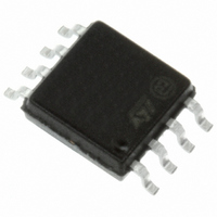
LCP02-150B1 STMicroelectronics, LCP02-150B1 Datasheet

LCP02-150B1
Specifications of LCP02-150B1
Available stocks
Related parts for LCP02-150B1
LCP02-150B1 Summary of contents
Page 1
... Both positive and negative threshold levels are programmable by two gates (Gn and Gp). The use of transistors decreases the battery currents during surge suppression. LCP02-150B1 can be used to help equipment to meet various standards such as UL1950, IEC 60950 / CSAC22.2, UL1459 and TIA-968-A (formerly FCC part68). A Trisil™ meets UL94 V0 (Trisils are UL497B approved - file: E136224) ...
Page 2
... A 800 10/560 µs type B 1000 9/720 µs Doc ID 7275 Rev 6 LCP02-150B1 Pin-out configuration NC GND GND NC Minimum Required Current serial resistor peak Waveform to meet current (A) standard (Ω) 500 2/10 µ ...
Page 3
... LCP02-150B1 Table 2. Absolute maximum ratings (T Symbol I Peak pulse current PP Non repetitive surge peak on-state current ( Hz) I value specified for each line TSM I TSM I value can be applied on both lines at the same time TSM (GND capability is twice the line I V max Maximum negative battery voltage range ...
Page 4
... Test conditions measured Gp/GND Gp/GND (1) 10/700 µ 1.2/50 µ Test conditions ° +120 LINE ° -120 LINE MHz Component Doc ID 7275 Rev 6 LCP02-150B1 Min. Max. Unit Ω Ω Min. Max GP/LINE = - GN/LINE = - Min. Typ. Max. 100 220 mA V Unit µA pF Unit nF ...
Page 5
... LCP02-150B1 Figure 4. Relative variation of holding current versus junction temperature 1.6 1.4 1.2 1.0 0.8 0.6 0.4 0.2 0.0 Figure 5. Maximum non repetitive surge peak on state current versus overload duration Figure 6. Capacitance versus reverse applied voltage (typical values) with V T (°C) -40 -20 ...
Page 6
... SLIC efficient they have close as possible to the LCP02 gate pins (Gn and Gp) and to the reference ground track (or plan). The optimized value for Cn and Cp is 220nF. 6/10 Rs1 Ign T1 Th1 -Vbat Gn Cn Rs2 RING also applies. Doc ID 7275 Rev 6 LCP02-150B1 TIP V Tip T2 Igp Th2 Gp +Vb Cp GND V Ring Figure 4 ...
Page 7
... Rs = series resistor of the line card (e.g. PTC) For a line card with 50 Ω of series resistors which has to be qualified under Bellcore 1000 V 10/1000 µs surge, the present current through the LCP02-150B1 is equal surge = 1000 / ( The LCP02-150B1 topology is particularly optimized for the new telecom applications such as fiber in the loop, WLL systems, decentralized central office for example ...
Page 8
... Figure 9. SO-8 wide footprint measurements in mm (inches) 8/ 4.33 (0.170) 8.38 (0.330) 0.52 (0.020) Doc ID 7275 Rev 6 LCP02-150B1 Dimensions Ref. Millimeters Min. Typ. Max. Min. A 2.50 A1 0.25 A2 1.51 2.00 0.059 b 0.35 0.40 0.51 0.013 0.016 0.020 c 0.10 0.20 0.35 0.003 0.008 0.014 D 6 ...
Page 9
... LCP02-150B1 4 Ordering information Table 9. Ordering information Order code LCP02-150B1RL 5 Revision history Table 10. Document revision history Date Revision Sep-2000 17-Oct-2008 28-Jun-2010 Marking Package LCP02 SO-8-Wide 4A Previous release. 5 Reformatted to current standards. V Removed 1 kV values for V 6 symbol and trademark statement for Trisil on the coverpage. Updated package dimension graphics ...
Page 10
... Australia - Belgium - Brazil - Canada - China - Czech Republic - Finland - France - Germany - Hong Kong - India - Israel - Italy - Japan - Malaysia - Malta - Morocco - Philippines - Singapore - Spain - Sweden - Switzerland - United Kingdom - United States of America 10/10 Please Read Carefully: © 2010 STMicroelectronics - All rights reserved STMicroelectronics group of companies www.st.com Doc ID 7275 Rev 6 LCP02-150B1 ...


