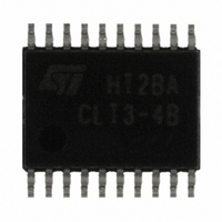
CLT3-4BT6-TR STMicroelectronics, CLT3-4BT6-TR Datasheet - Page 7

CLT3-4BT6-TR
Manufacturer Part Number
CLT3-4BT6-TR
Description
TERMINATION QUAD DGTL TSSOP-20
Manufacturer
STMicroelectronics
Type
Digital Terminationr
Datasheet
1.CLT3-4BT6-TR.pdf
(13 pages)
Specifications of CLT3-4BT6-TR
Technology
Mixed Technology
Number Of Circuits
4
Applications
General Purpose
Package / Case
20-TSSOP
Diode Type
ESD Protection
Clamping Voltage Vc Max
38V
Operating Voltage
10V
Diode Case Style
TSSOP
No. Of Pins
20
Operating Supply Voltage
10 V
Supply Current
0.0008 A
Maximum Operating Temperature
+ 85 C
Minimum Operating Temperature
- 25 C
Mounting Style
SMD/SMT
For Use With
497-6401 - BOARD EVAL FOR CLT3-4
Lead Free Status / RoHS Status
Lead free / RoHS Compliant
Power (watts)
-
Voltage - Working
-
Voltage - Clamping
-
Lead Free Status / Rohs Status
Details
Other names
497-2455-2
Available stocks
Company
Part Number
Manufacturer
Quantity
Price
Part Number:
CLT3-4BT6-TR
Manufacturer:
ST
Quantity:
20 000
CLT3-4B
2
2.1
2.2
Application information
Application description
The CLT device is used between the input module and the opto-coupler of an I/O module. To
secure the coupler off state and the non-conduction of its diode, the maximum CLT output
current is 40 µA with R opto = 15 kΩ. When the CLT input voltage V
minimum CLT output current of 1.5 mA will secure the opto-coupler on state.
The CLT limiter is insensitive to the output voltage up to 2.0V. Therefore, its output is able to
drive any state of the art opto-coupler. Some additional device can be added in series with
the opto-coupler if the output voltage remains within its functional limits.
A stand-alone sensor is normally connected on the CLT input. For a good off state control,
its quiescent current has to be less than 1.5 mA (EN60947-5-2 standard compatible)
keeping then the opto-coupler off thanks to the CLT device (I
ON state voltage V
corresponding to the difference between the minimum supply voltage (V
and the maximum current limitation activation voltage:
V
V
(V
Input reverse polarity robustness
Each input of the CLT device may be biased to a reverse polarity. This case corresponds to
a connection mistake or a reverse biasing that is generated by the demagnetization of a
monitored inductive solenoid.
The involved input can withstand the reverse current up to 20 mA (in the configuration
shown in
Such a case is not critical for the CLT3-4 itself, as it represents less than 15 mW per
disturbed input. But the input resistors should be designed with care regardless of their
thermal characteristics (refer to Application note AN2527).
When the reverse polarity operation is required in types 3 input mode, it is recommended to
increase the input resistance R
input current below its maximum allowed level (20 mA). The surge and transient immunity
robustness of the CLT3 is then also increased.
A 1.8 kΩ value allows the reverse input current to be reduced to 16.2 mA and the resistor
dissipation to be reduced to 0.47 W, for 30 V V
The CLT3 normal operation in type 3 is fully compatible with this recommended resistance
since its internal state threshold is monitored at V
V
In type 1 input operation where R
0.39 W.
The other inputs remain operational, as long as the power supply is working properly
(V
CC MIN
I
I
I
CC
= V
= 11 V and V
= 11 V when V
>19 V). Refer to Application note AN 2527 for representative application design case.
IN
= V
+ R
Figure
S-ON
I
x I
IN MAX
CC
10) through its input protection diode while its opto-coupler remains OFF.
+ V
IN
S-ON
= 19 V.
I
= 5 V, R
will be lower than 8 V (EN60947-5-2 standard compatible)
I
= 1.2 kΩ, I
I
to 1.8 kΩ in order to reduce its dissipation and keep the
I
= 2.2 kΩ the dissipation of this resistor is less than
IN
< 3.7 mA).
CC
IN
and a - 30 V V
= 4.2 V and V
OUT
< 40 µA). And its maximum
I
C
voltages.
Application information
= 10V - corresponding to
IN
is higher than 5 V, a
CC MIN
= 19.2 V)
7/13


