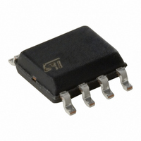
L4931CD33 STMicroelectronics, L4931CD33 Datasheet - Page 17

L4931CD33
Manufacturer Part Number
L4931CD33
Description
IC REG VLDO 250MA 3.3V 8-SOIC
Manufacturer
STMicroelectronics
Specifications of L4931CD33
Regulator Topology
Positive Fixed
Voltage - Output
3.3V
Voltage - Input
Up to 20V
Voltage - Dropout (typical)
0.4V @ 250mA
Number Of Regulators
1
Current - Output
250mA
Operating Temperature
-40°C ~ 125°C
Mounting Type
Surface Mount
Package / Case
8-SOIC (3.9mm Width)
Primary Input Voltage
5.3V
Output Voltage Fixed
3.3V
Dropout Voltage Vdo
400mV
No. Of Pins
8
Output Current
300mA
Voltage Regulator Case Style
SOIC
Operating Temperature Range
-40°C To +85°C
Rohs Compliant
Yes
Lead Free Status / RoHS Status
Lead free / RoHS Compliant
Current - Limit (min)
-
Available stocks
Company
Part Number
Manufacturer
Quantity
Price
Part Number:
L4931CD33
Manufacturer:
ST
Quantity:
20 000
Company:
Part Number:
L4931CD33-TR
Manufacturer:
STMicroelectronics
Quantity:
39 741
Part Number:
L4931CD33-TR
Manufacturer:
ST
Quantity:
20 000
Part Number:
L4931CD33-TRY
Manufacturer:
ST
Quantity:
20 000
Company:
Part Number:
L4931CD33TRY
Manufacturer:
ST
Quantity:
3 748
ELECTRICAL CHARACTERISTICS OF L4931Cxx55 (refer to the test circuits, T
C
(*) For SO-8 package the maximum limit of load regulation and dropout is increased by 20 mV.
ELECTRICAL CHARACTERISTICS OF L4931ABxx60 (refer to the test circuits, T
C
(*) For SO-8 package the maximum limit of load regulation and dropout is increased by 20 mV.
Symbol
Symbol
I
I
V
V
SVR
SVR
V
V
= 0.1 µF, C
= 0.1 µF, C
V
V
V
I
V
C
V
I
V
C
eN
eN
V
out
d
V
out
d
V
I
V
I
I
I
O
O
d
IH
d
IH
O
(*)
IL
I
O
(*)
IL
I
O
O
I
I
O
O
(*)
(*)
Output Voltage
Operating Input Voltage
Output Current Limit
Line Regulation
Load Regulation
Quiescent Current
ON MODE
OFF MODE
Supply Voltage Rejection
Output Noise Voltage
Dropout Voltage
Control Input Logic Low
Control Input Logic High
Control Input Current
Output Bypass Capacitance ESR = 0.1 to 10
O
O
= 2.2 µF unless otherwise specified).
= 2.2 µF unless otherwise specified).
Parameter
Parameter
I
I
I
V
V
V
V
V
I
V
B =10 Hz to 100 KHz
I
I
T
T
V
I
I
I
V
V
V
V
V
I
V
B =10 Hz to 100 KHz
I
I
T
T
V
O
O
O
O
O
O
O
O
O
O
O
O
A
A
A
A
I
I
I
I
I
I
I
I
I
I
I
I
I
I
= -40 to 125°C
= -40 to 125°C
= -40 to 125°C
= -40 to 125°C
= 6.3 to 20 V
= 6.5 V
= 6.5 to 20 V
= 6.5 to 20 V
= 6 V
= 7.5 ± 1 V
= 6 V,
= 6.8 to 20 V
= 7 V
= 7 to 20 V
= 7 to 20 V
= 6 V
= 8 ± 1 V
= 6 V,
= 5 mA
= 5 mA
= 250 mA
= 5 mA
= 250 mA
= 250 mA
= 5 mA
= 5 mA
= 250 mA
= 5 mA
= 250 mA
= 250 mA
Test Conditions
Test Conditions
V
V
V
V
V
V
I
I
C
I
I
C
= 7.5 V
= 7.5 V
= 8 V
= 8 V
= 6 V
= 6 V
I
I
I
I
T
I
I
I
I
T
O
O
O
O
O
O
O
O
J
J
f = 120 Hz
f = 1 KHz
f = 10 KHz
f = 120 Hz
f = 1 KHz
f = 10 KHz
= -40 to 125°C
= -40 to 125°C
= 0.5 mA
= 0.5 to 250 mA
= 0 mA
= 250 mA
= 0.5 mA
= 0.5 to 250 mA
= 0 mA
= 250 mA
I
I
O
O
= 0 to 250 mA
= 0 to 250 mA
T
T
A
A
=-25 to 85°C
=-25 to 85°C
Min.
5.39
5.28
Min.
5.94
5.88
2
2
2
2
J
= 25°C,
J
Typ.
Typ.
300
300
5.5
3.5
0.6
0.4
0.8
4.5
0.4
50
70
67
55
50
10
10
70
69
66
55
50
10
10
3
4
6
4
3
= 25°C,
L4931 SERIES
Max.
Max.
5.61
5.72
6.06
6.12
100
140
0.6
0.8
0.8
1.6
0.6
0.8
0.8
20
21
18
20
20
15
1
6
7
Unit
Unit
mA
mV
mV
mA
mA
mV
mV
mA
µA
µA
µA
µA
dB
µF
dB
µF
17/29
V
V
V
V
V
V
V
V
V
V
V
V


