C650-260-WH Bourns Inc., C650-260-WH Datasheet

SURGE SUPP TBU 260MA 650VIMP SMD

C650-260-WH

Manufacturer Part Number
C650-260-WH
Description
SURGE SUPP TBU 260MA 650VIMP SMD
Manufacturer
Bourns Inc.
Series
TBU™r
Datasheets

Specifications of C650-260-WH

Voltage - Working
300V
Technology
Mixed Technology
Number Of Circuits
1
Applications
General Purpose
Package / Case
0.325" L x 0.157 " W x 0.033" H (8.25mm x 4mm x 0.85mm)
Voltage Rating
14 V
Current Rating
260 mA
Height
0.85 mm
Length
8.25 mm
Mounting
SMD/SMT
Operating Temperature Range
- 40 C to + 85 C
Termination Style
SMD/SMT
Width
4 mm
Suppressor Type
Data Line / Mains
Output Current
520mA
Peak Surge Current
260mA
Response Time
1µs
Resistance
8ohm
Operating Temperature Max
85°C
Clamping Voltage Vc Max
650V
Length/height, External
0.85mm
Rohs Compliant
Yes
External Depth
4mm
External Width
8.25mm
Lead Free Status / RoHS Status
Lead free / RoHS Compliant
Power (watts)
-
Voltage - Clamping
-
Lead Free Status / Rohs Status
Lead free / RoHS Compliant

Available stocks

Company
Part Number
Manufacturer
Quantity
Price
Part Number:
C650-260-WH
Manufacturer:
FULTEC
Quantity:
200
Bourns
bidirectional protection components, constructed using
MOSFET semiconductor technology, designed to protect
against faults caused by short circuits, AC power cross,
induction and lightning surges.
The TBU
the MOSFET, blocks surges and provides an effective barrier
behind which sensitive electronics are not exposed to large
voltages or currents during surge events. The TBU
provided in a surface mount DFN package and meets industry
standard requirements such as RoHS and Pb Free solder
refl ow profi les.
*RoHS Directive 2002/95/EC Jan 27, 2003 including Annex.
Specifi cations are subject to change without notice.
Customers should verify actual device performance in their specifi c applications.
C650 and C850 TBU
Symbol
I
I
I
R
t
I
V
Symbol
V
V
T
T
op
trigger
out
quiescent
block
Transient Blocking Units - TBU
Electrical Characteristics (T
Absolute Maximum Ratings (T
reset
imp
rms
op
stg
device
®
®
C650 and C850 series products are high speed
high speed protector, triggering as a function of
Parameter
Maximum protection voltage for impulse faults with rise time ≥ 1 µsec
Maximum protection voltage for continuous V
Operating temperature range
Storage temperature range
Parameter
Maximum current through the device that will not cause
current blocking
Typical current for the device to go from normal operating
state to protected state
Maximum current through the device
Series resistance of the TBU
Maximum time for the device to go from normal operating
state to protected state
Current through the triggered TBU
voltage
Voltage below which the triggered TBU
normal operating state
®
protectors are bidirectional; specifi cations are valid in both directions.
amb
amb
®
= 25 °C)
Devices
= 25 °C)
®
device
TBU
®
Features
device with 50 Vdc circuit
Formerly
Extremely high speed performance
Blocks high voltages and currents
Very high bandwidth; GHz compatible
Small package, minimal PCB area
Simple, superior circuit protection
RoHS compliant*, UL Recognized
®
®
device is
device will transition to
®
C650 and C850 Protectors
rms
faults
brand
UL recognized component File # E315805.
Telcordia
ITU-T
Agency Approval
Industry Standards
Cx50-100-WH
Cx50-180-WH
Cx50-260-WH
Cx50-100-WH
Cx50-180-WH
Cx50-260-WH
Cx50-100-WH
Cx50-180-WH
Cx50-260-WH
C650-100-WH
C650-180-WH
C650-260-WH
C850-100-WH
C850-180-WH
C850-260-WH
C650-xxx-WH
C850-xxx-WH
C650-xxx-WH
C850-xxx-WH
GR-1089
GR-974
K.20, K.20E, K.21, K.21E, K.45
Description
Min.
The C650 & C850 Series are currently
Port Type 1, 3, 5
available, but not recommended for
new designs. Bourns
-65 to +150
-40 to +85
Typ.
Series
150
220
330
12
17
11
11
14
8
8
1
Value
650
850
300
425
is preferred.
Max.
14.5
100
180
260
200
360
520
10
10
19
14
14
1
®
TBU-CA
Unit
°C
°C
Model
V
V
C650
C850
C650
C850
C850
Unit
mA
mA
mA
mA
µs
Ω
V

Related parts for C650-260-WH

C650-260-WH Summary of contents

Page 1

... Cx50-100-WH Cx50-180-WH Cx50-260-WH Cx50-100-WH Cx50-180-WH Cx50-260-WH Cx50-100-WH Cx50-180-WH Cx50-260-WH C650-100-WH C650-180-WH C650-260-WH ® device C850-100-WH C850-180-WH C850-260-WH ® device with 50 Vdc circuit ® device will transition to The C650 & C850 Series are currently available, but not recommended for new designs. Bourns Series is preferred ...

Page 2

... Voice linecards ■ MDF, primary protection modules ■ Process control equipment ■ Test and measurement equipment ■ General electronics ® TBU C650 and C850 Protectors Typical Performance Characteristics V-I Characteristics +I I trigger -V reset V reset -I trigger Current vs. Temperature 140 120 100 ...

Page 3

... TEST CONFIGURATION DIAGRAM C650 Lightning, 650 µs/div. Ch1 V1 Ch2 V2 C650 Power Fault, 300 Vrms, 100 ms/div. Ch1 V1 Ch2 V2 Specifi cations are subject to change without notice. Customers should verify actual device performance in their specifi c applications. ® ...

Page 4

... TBU C650 and C850 Protectors Product Dimensions PIN 1 TOP VIEW SIDE VIEW Recommended Pad Layout 1.15 (.045) 0.70 (.028) 2.625 (.103) 3.55 (.140) TBU ® protectors have matte-tin termination fi nish. Suggested layout should use non-solder mask defi ne (NSMD). Recommended stencil thickness is 0 ...

Page 5

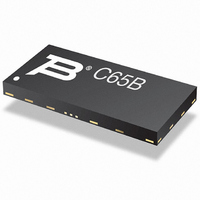
... MANUFACTURER’S MARKING NUMBER TRADEMARK* C65A = C650-100-WH C65B = C650-180-WH C65C = C650-260-WH C85A = C850-100-WH C85B = C850-180-WH C85C = C850-260-WH PIN 1 MANUFACTURING DATE CODE* - 1ST DIGIT INDICATES THE YEAR’S 6-MONTH PERIOD. - 2ND DIGIT INDICATES THE WEEK NUMBER IN THE 6-MONTH PERIOD. ...

Page 6

... TBU C650 and C850 Protectors Reference Application The C-series devices are general use protectors used in a wide variety of applications. The following diagram is one common confi guration example of C-series device placement. A cost-effective protection solution combines Bourns devices with a pair of MOVs or Bourns ® ...

Related keywords