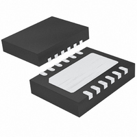
LT4356HDE-3#PBF Linear Technology, LT4356HDE-3#PBF Datasheet

LT4356HDE-3#PBF
Specifications of LT4356HDE-3#PBF
Related parts for LT4356HDE-3#PBF
LT4356HDE-3#PBF Summary of contents
Page 1
... High Side Switch for Battery Powered Systems n Intrinsic Safety Applications L, LT, LTC, LTM, Linear Technology and the Linear logo are registered trademarks of Linear Technology Corporation. All other trademarks are the property of their respective owners. TYPICAL APPLICATION 4A, 12V Overvoltage Output Regulator 10mΩ ...
Page 2
... PLASTIC DFN T = 125°C, θ = 43°C/W JMAX JA EXPOSED PAD (PIN 13) PCB GND CONNECTION OPTIONAL ORDER INFORMATION LEAD FREE FINISH TAPE AND REEL LT4356CDE-3#PBF LT4356CDE-3#TRPBF LT4356IDE-3#PBF LT4356IDE-3#TRPBF LT4356HDE-3#PBF LT4356HDE-3#TRPBF LT4356CMS-3#PBF LT4356CMS-3#TRPBF LT4356IMS-3#PBF LT4356IMS-3#TRPBF LT4356HMS-3#PBF LT4356HMS-3#TRPBF LT4356CS-3#PBF LT4356CS-3#TRPBF LT4356IS-3#PBF LT4356IS-3#TRPBF LT4356HS-3#PBF LT4356HS-3#TRPBF ...
Page 3
ORDER INFORMATION LEAD BASED FINISH TAPE AND REEL LT4356IMS-3 LT4356IMS-3#TR LT4356HMS-3 LT4356HMS-3#TR LT4356CS-3 LT4356CS-3#TR LT4356IS-3 LT4356IS-3#TR LT4356HS-3 LT4356HS-3#TR Consult LTC Marketing for parts specifi ed with wider operating temperature ranges. *The temperature grade is identifi label on ...
Page 4
LT4356-3 ELECTRICAL CHARACTERISTICS temperature range, otherwise specifi cations are at T SYMBOL PARAMETER I OUT Pin Input Current OUT ΔV OUT Pin High Threshold OUT SHDN Pin Threshold V SHDN SHDN Pin Float Voltage V SHDN(FLT) SHDN Pin Current I ...
Page 5
TYPICAL PERFORMANCE CHARACTERISTICS Specifi cations are 12V 25°C unless otherwise noted SHDN Current vs Temperature SHDN –50 – 100 ...
Page 6
LT4356-3 TYPICAL PERFORMANCE CHARACTERISTICS Specifi cations are 12V 25°C unless otherwise noted Overcurrent TMR Current vs (V – OUT 280 OVERCURRENT CONDITION OUT 240 ...
Page 7
PIN FUNCTIONS A (DFN and SO Packages Only): Amplifi er Output. OUT Open collector output of the auxiliary amplifi er capable of sinking up to 2mA from 80V. The negative input of the amplifi internally connected ...
Page 8
LT4356-3 BLOCK DIAGRAM 50mV – SHDN A OUT – 1.25V AUXILIARY AMPLIFIER + + IN 8 SNS GATE 14V CHARGE PUMP – OC OUT SHDN CONTROL LOGIC GATEOFF – 1.35V 0.5V + ...
Page 9
OPERATION Some power systems must cope with high voltage surges of short duration such as those in automobiles. Load circuitry must be protected from these transients, yet high availability systems must continue operating during these events. The LT4356 ...
Page 10
LT4356-3 APPLICATIONS INFORMATION The LT4356-3 can limit the voltage and current to the load circuitry during supply transients or overcurrent events. The total fault timer period should be set to ride through short overvoltage transients while not causing damage to ...
Page 11
APPLICATIONS INFORMATION Fault Timer Current The timer current starts at around 2μA with 0.5V or less increasing linearly to 50μA with 75V ing an overvoltage fault (Figure 1). During an overcurrent fault, it starts ...
Page 12
LT4356-3 APPLICATIONS INFORMATION This fi xed early warning period allows time for the system to perform necessary backup or house-keeping functions before power is cut off. When V TMR threshold, the GATE pin pulls low immediately and turns off the ...
Page 13
APPLICATIONS INFORMATION MOSFET stress is the result of power dissipated within the device. For long duration surges of 100ms or more, stress is increasingly dominated by heat transfer; this is a matter of device packaging and mounting, and heatsink thermal ...
Page 14
LT4356-3 APPLICATIONS INFORMATION The LT4356-3 does not need extra compensation compo- nents at the GATE pin for stability during an overvoltage or overcurrent event. However, with fast, high voltage transient steps at the input, a gate capacitor, C1, to ground ...
Page 15
APPLICATIONS INFORMATION SNS 10mΩ Si4435 IRLR2908 V IN 12V D1 D2* 1N5245 SMAJ58CA 15V R6 10k 5 4 SNS GATE LT4356DE-3 7 SHDN 11 A OUT GND TMR ...
Page 16
LT4356-3 APPLICATIONS INFORMATION First, calculate the resistive divider value to limit V 16V during an overvoltage event 1.25V • 16V = REG R2 Set the current through R1 and R2 during the overvoltage ...
Page 17
TYPICAL APPLICATIONS Wide Input Range 5V to 28V Hot Swap with Undervoltage Lockout 24V D2* SMAT70A *DIODES INC SNS 0.02Ω SUD50N03- 118k 10Ω SNS GATE OUT CC 47nF SHDN A ...
Page 18
LT4356-3 TYPICAL APPLICATIONS Overvoltage Regulator with Low Battery Detection and Output Keep Alive During Shutdown V IN 12V D2* SMAJ58A 2.5A, 48V Hot Swap with Overvoltage Output Regulation at 72V and UV Shutdown at 35V V IN 48V D2* SMAT70A ...
Page 19
TYPICAL APPLICATIONS 2.5A, 28V Hot Swap with Overvoltage Output Regulation at 36V and UV Shutdown at 15V V IN 28V D2* SMAT70A Overvoltage Regulator with Reverse Input Protection Up to –80V V IN 12V D1 1N4148 *DIODES INC. **OPTIONAL COMPONENT ...
Page 20
LT4356-3 3.60 0.05 2.20 0.05 1.70 0.05 0.25 0.05 RECOMMENDED SOLDER PAD PITCH AND DIMENSIONS APPLY SOLDER MASK TO AREAS THAT ARE NOT SOLDERED PIN 1 TOP MARK (NOTE 6) 0.200 REF NOTE: 1. DRAWING PROPOSED VARIATION ...
Page 21
Plastic MSOP (Reference LTC DWG # 05-08-1661) 0.889 ± 0.127 (.035 ± .005) 5.23 3.20 – 3.45 (.206) (.126 – .136) MIN 0.305 ± 0.038 0.50 (.0120 ± .0015) (.0197) TYP BSC RECOMMENDED SOLDER PAD LAYOUT DETAIL “A” 0.254 ...
Page 22
LT4356-3 PACKAGE DESCRIPTION .050 BSC N .245 MIN .030 .005 TYP RECOMMENDED SOLDER PAD LAYOUT .010 – .020 45 (0.254 – 0.508) .008 – .010 (0.203 – 0.254) .016 – .050 (0.406 – 1.270) NOTE: INCHES 1. ...
Page 23
... Text Added to Applications Information Update Typical Applications Information furnished by Linear Technology Corporation is believed to be accurate and reliable. However, no responsibility is assumed for its use. Linear Technology Corporation makes no representa- tion that the interconnection of its circuits as described herein will not infringe on existing patent rights. LT4356-3 ...
Page 24
... ADC and I C LTC4352 Ideal MOSFET ORing Diode LTC4354 Negative Voltage Diode-OR Controller LTC4355 Positive Voltage Diode-OR Controller Hot Swap and ThinSOT are trademarks of Linear Technology Corporation. SENSE Linear Technology Corporation 24 1630 McCarthy Blvd., Milpitas, CA 95035-7417 (408) 432-1900 FAX: (408) 434-0507 ● Q2 ...


