LM2931T-5.0G ON Semiconductor, LM2931T-5.0G Datasheet - Page 23
LM2931T-5.0G
Manufacturer Part Number
LM2931T-5.0G
Description
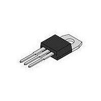
IC REG LDO 100MA 5V TO220AB
Manufacturer
ON Semiconductor
Datasheet
1.LM2931AZ-5.0RAG.pdf
(23 pages)
Specifications of LM2931T-5.0G
Regulator Topology
Positive Fixed
Voltage - Output
5V
Voltage - Input
Up to 40V
Voltage - Dropout (typical)
0.16V @ 100mA
Number Of Regulators
1
Current - Output
100mA
Operating Temperature
-40°C ~ 125°C
Mounting Type
Through Hole
Package / Case
TO-220-3 (Straight Leads)
Number Of Outputs
1
Polarity
Positive
Input Voltage Max
40 V
Output Voltage
5 V
Output Type
Fixed
Dropout Voltage (max)
0.2 V at 10 mA
Output Current
100 mA
Line Regulation
30 mV
Load Regulation
50 mV
Voltage Regulation Accuracy
5 %
Maximum Operating Temperature
+ 125 C
Mounting Style
Through Hole
Minimum Operating Temperature
- 40 C
Primary Input Voltage
40V
Output Voltage Fixed
5V
Dropout Voltage Vdo
600mV
No. Of Pins
3
Operating Temperature Range
-40°C To +150°C
Filter Terminals
Through Hole
Rohs Compliant
Yes
Current Rating
0.1A
Lead Free Status / RoHS Status
Lead free / RoHS Compliant
Current - Limit (min)
-
Lead Free Status / Rohs Status
Lead free / RoHS Compliant
Other names
LM2931T-5.0GOS
Available stocks
Company
Part Number
Manufacturer
Quantity
Price

Part Number:
LM2931T-5.0G
Manufacturer:
ON/安森美
Quantity:
20 000


PUBLICATION ORDERING INFORMATION
LITERATURE FULFILLMENT:
Literature Distribution Center for ON Semiconductor
P.O. Box 5163, Denver, Colorado 80217 USA
Phone: 303−675−2175 or 800−344−3860 Toll Free USA/Canada
Fax: 303−675−2176 or 800−344−3867 Toll Free USA/Canada
Email: orderlit@onsemi.com
ON Semiconductor and
to any products herein. SCILLC makes no warranty, representation or guarantee regarding the suitability of its products for any particular purpose, nor does SCILLC assume any liability
arising out of the application or use of any product or circuit, and specifically disclaims any and all liability, including without limitation special, consequential or incidental damages.
“Typical” parameters which may be provided in SCILLC data sheets and/or specifications can and do vary in different applications and actual performance may vary over time. All
operating parameters, including “Typicals” must be validated for each customer application by customer’s technical experts. SCILLC does not convey any license under its patent rights
nor the rights of others. SCILLC products are not designed, intended, or authorized for use as components in systems intended for surgical implant into the body, or other applications
intended to support or sustain life, or for any other application in which the failure of the SCILLC product could create a situation where personal injury or death may occur. Should
Buyer purchase or use SCILLC products for any such unintended or unauthorized application, Buyer shall indemnify and hold SCILLC and its officers, employees, subsidiaries, affiliates,
and distributors harmless against all claims, costs, damages, and expenses, and reasonable attorney fees arising out of, directly or indirectly, any claim of personal injury or death
associated with such unintended or unauthorized use, even if such claim alleges that SCILLC was negligent regarding the design or manufacture of the part. SCILLC is an Equal
Opportunity/Affirmative Action Employer. This literature is subject to all applicable copyright laws and is not for resale in any manner.
0.010 (0.254)
B
K
D
M
C
T
1 2 3
are registered trademarks of Semiconductor Components Industries, LLC (SCILLC). SCILLC reserves the right to make changes without further notice
A
4 5
G
S
*For additional information on our Pb−Free strategy and soldering
H
10.66
details, please download the ON Semiconductor Soldering and
Mounting Techniques Reference Manual, SOLDERRM/D.
OPTIONAL
CHAMFER
0.42
N
R
N. American Technical Support: 800−282−9855 Toll Free
Europe, Middle East and Africa Technical Support:
Japan Customer Focus Center
PACKAGE DIMENSIONS
SOLDERING FOOTPRINT*
USA/Canada
Phone: 421 33 790 2910
Phone: 81−3−5773−3850
8.38
0.33
−T−
http://onsemi.com
M
E
CASE 936A−02
D2T SUFFIX
ISSUE C
L
D
16.02
0.63
2
PAK
23
V
P
TERMINAL 6
U
3.05
0.12
SCALE 3:1
1.702
0.067
NOTES:
1. DIMENSIONING AND TOLERANCING PER ANSI
2. CONTROLLING DIMENSION: INCH.
3. TAB CONTOUR OPTIONAL WITHIN DIMENSIONS A
4. DIMENSIONS U AND V ESTABLISH A MINIMUM
5. DIMENSIONS A AND B DO NOT INCLUDE MOLD
inches
mm
Y14.5M, 1982.
AND K.
MOUNTING SURFACE FOR TERMINAL 6.
FLASH OR GATE PROTRUSIONS. MOLD FLASH
AND GATE PROTRUSIONS NOT TO EXCEED 0.025
(0.635) MAXIMUM.
1.016
0.04
DIM
G
M
A
B
C
D
E
H
K
L
N
P
R
S
U
V
ON Semiconductor Website: www.onsemi.com
Order Literature: http://www.onsemi.com/orderlit
For additional information, please contact your local
Sales Representative
0.386
0.356
0.170
0.026
0.045
0.539
0.000
0.088
0.018
0.058
MIN
0.067 BSC
0.050 REF
0.116 REF
0.200 MIN
0.250 MIN
5 REF
INCHES
_
0.403
0.368
0.180
0.036
0.055
0.579
0.010
0.102
0.026
0.078
MAX
13.691
9.804
9.042
4.318
0.660
1.143
0.000
2.235
0.457
1.473
MILLIMETERS
MIN
1.702 BSC
1.270 REF
2.946 REF
5.080 MIN
6.350 MIN
5 REF
_
10.236
14.707
MAX
9.347
4.572
0.914
1.397
0.254
2.591
0.660
1.981
LM2931/D
Related parts for LM2931T-5.0G
Image
Part Number
Description
Manufacturer
Datasheet
Request
R

Part Number:
Description:
IC REG LDO 100MA 5V TO220AB
Manufacturer:
ON Semiconductor
Datasheet:

Part Number:
Description:
Low power dual voltage comparator
Manufacturer:
STMicroelectronics
Datasheet:
Part Number:
Description:
ON Semiconductor [VOLTAGE REGULATOR]
Manufacturer:
ON Semiconductor
Datasheet:
Part Number:
Description:
357-036-542-201 CARDEDGE 36POS DL .156 BLK LOPRO
Manufacturer:
ON Semiconductor
Datasheet:
Part Number:
Description:
357-036-542-201 CARDEDGE 36POS DL .156 BLK LOPRO
Manufacturer:
ON Semiconductor
Datasheet:
Part Number:
Description:
357-036-542-201 CARDEDGE 36POS DL .156 BLK LOPRO
Manufacturer:
ON Semiconductor
Datasheet:
Part Number:
Description:
357-036-542-201 CARDEDGE 36POS DL .156 BLK LOPRO
Manufacturer:
ON Semiconductor
Datasheet:
Part Number:
Description:
357-036-542-201 CARDEDGE 36POS DL .156 BLK LOPRO
Manufacturer:
ON Semiconductor
Datasheet:
Part Number:
Description:
357-036-542-201 CARDEDGE 36POS DL .156 BLK LOPRO
Manufacturer:
ON Semiconductor
Datasheet:
Part Number:
Description:
357-036-542-201 CARDEDGE 36POS DL .156 BLK LOPRO
Manufacturer:
ON Semiconductor
Datasheet:
Part Number:
Description:
357-036-542-201 CARDEDGE 36POS DL .156 BLK LOPRO
Manufacturer:
ON Semiconductor
Datasheet:
Part Number:
Description:
357-036-542-201 CARDEDGE 36POS DL .156 BLK LOPRO
Manufacturer:
ON Semiconductor
Datasheet:
Part Number:
Description:
357-036-542-201 CARDEDGE 36POS DL .156 BLK LOPRO
Manufacturer:
ON Semiconductor
Datasheet:
Part Number:
Description:
Manufacturer:
ON Semiconductor
Datasheet: