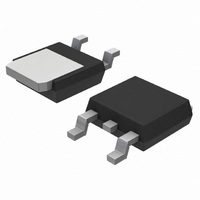
LP2950ACDT-5RKG ON Semiconductor, LP2950ACDT-5RKG Datasheet - Page 6

LP2950ACDT-5RKG
Manufacturer Part Number
LP2950ACDT-5RKG
Description
IC REG LDO LP 100MA 5V DPAK-4
Manufacturer
ON Semiconductor
Datasheet
1.LP2951ACDR2G.pdf
(23 pages)
Specifications of LP2950ACDT-5RKG
Regulator Topology
Positive Fixed
Voltage - Output
5V
Voltage - Input
Up to 30V
Voltage - Dropout (typical)
0.35V @ 100mA
Number Of Regulators
1
Current - Output
100mA
Operating Temperature
-40°C ~ 125°C
Mounting Type
Surface Mount
Package / Case
TO-252-2, DPak (2 Leads + Tab), TO-252AA, SC-63
Lead Free Status / RoHS Status
Lead free / RoHS Compliant
Current - Limit (min)
-
Other names
LP2950ACDT-5RKG
LP2950ACDT-5RKGOSTR
LP2950ACDT-5RKGOSTR
Available stocks
Company
Part Number
Manufacturer
Quantity
Price
Part Number:
LP2950ACDT-5RKG
Manufacturer:
ON/安森美
Quantity:
20 000
at which the regulator output no longer maintains regulation
against further reductions in input voltage. Measured when
the output drops 100 mV below its nominal value (which is
measured at 1.0 V differential), dropout voltage is affected
by junction temperature, load current and minimum input
supply requirements.
change in input voltage. The measurement is made under
conditions of low dissipation or by using pulse techniques
such that average chip temperature is not significantly
affected.
change in load current at constant chip temperature.
device dissipation for which the regulator will operate
within specifications.
regulator chip and is not delivered to the load.
Dropout Voltage − The input/output voltage differential
Line Regulation − The change in output voltage for a
Load Regulation − The change in output voltage for a
Maximum Power Dissipation − The maximum total
Bias Current − Current which is used to operate the
0.01
5.00
4.99
4.98
4.97
4.96
4.95
1.0
0.1
10
0.1
- 50
Figure 4. Output Voltage versus Temperature
0
Figure 2. Quiescent Current
T
A
, AMBIENT TEMPERATURE (°C)
1.0
I
L
, LOAD CURRENT (mA)
50
100
10
150
LP2951C
http://onsemi.com
DEFINITIONS
100
200
6
output, with constant load and no input ripple, measured
over a specified frequency range.
transistor collector−base junction, under a specified
collector voltage, when the transistor is “off”.
comparator input terminal, below the reference voltage
which is applied to the other comparator input terminal,
which causes the comparator output to change state from a
logic “0” to “1”.
comparator input terminal, below the reference voltage
which is applied to the other comparator input terminal,
which causes the comparator output to change state from a
logic “1” to “0”.
voltage and Upper Threshold voltage.
Output Noise Voltage − The RMS ac voltage at the
Leakage Current − Current drawn through a bipolar
Upper Threshold Voltage − Voltage applied to the
Lower Threshold Voltage − Voltage applied to the
Hysteresis − The difference between Lower Threshold
6.0
5.0
4.0
3.0
2.0
1.0
6.0
5.0
4.0
3.0
2.0
1.0
0
0
0
0
125°C
Figure 3. 5.0 V Dropout Characteristics over
Figure 5. 5.0 V Dropout Characteristics with
T
LP2951C
A
LP2951C
25°C
= 25°C
1.0
1.0
−40°C
2.0
2.0
V
V
in
in
, INPUT VOLTAGE (V)
, INPUT VOLTAGE (V)
R
L
R
Load
= 50 W
L
3.0
3.0
= 50 kW
R
L
= 50 W
4.0
4.0
5.0
5.0
6.0
6.0


