LM2991SX/NOPB National Semiconductor, LM2991SX/NOPB Datasheet - Page 3
LM2991SX/NOPB
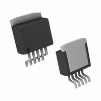
Manufacturer Part Number
LM2991SX/NOPB
Description
IC REG ADJ NEG LDO TO-263-5
Manufacturer
National Semiconductor
Specifications of LM2991SX/NOPB
Regulator Topology
Negative Adjustable
Voltage - Output
-3 ~ -24 V
Voltage - Input
0.3 ~ -26 V
Voltage - Dropout (typical)
0.6V @ 1A
Number Of Regulators
1
Current - Output
1A
Current - Limit (min)
1.5A
Operating Temperature
-40°C ~ 125°C
Mounting Type
Surface Mount
Package / Case
TO-263-5, D²Pak (5 leads + Tab), TO-263BA
Voltage Regulator Type
Linear
Topology
LDO
Regulator Output Type
Adjustable
Polarity Type
Negative
Number Of Outputs
Single
Input Voltage (min)
-26V
Input Voltage (max)
0.3V
Output Voltage
-3 to -24V
Package Type
TO-263
Output Current
1A
Load Regulation
0.4%
Line Regulation
0.04%/V
Operating Temp Range
-40C to 125C
Operating Temperature Classification
Automotive
Dropout Voltage@current (max)
0.2@100mA/0.8@1A
Dropout Voltage@current (typ)
0.1@100mA/0.6@1A
Pin Count
5 +Tab
Mounting
Surface Mount
Quiescent Current (max)
5mA
Polarity
Negative
Input Voltage Max
0.3 V
Output Type
Adjustable
Dropout Voltage (max)
0.6 V
Maximum Operating Temperature
+ 125 C
Mounting Style
Through Hole
Minimum Operating Temperature
- 40 C
Reference Voltage
- 1.186 V
Lead Free Status / RoHS Status
Lead free / RoHS Compliant
Other names
*LM2991SX
*LM2991SX/NOPB
LM2991SX
LM2991SX
LM2991SXTR
*LM2991SX/NOPB
LM2991SX
LM2991SX
LM2991SXTR


Reference Voltage
Output Voltage Range
Line Regulation
Load Regulation
Dropout Voltage
Quiescent Current
Dropout Quiescent Current V
Ripple Rejection
Output Noise
ON /OFF Input Voltage
ON /OFF Input Current
Output Leakage Current
Current Limit
Absolute Maximum Ratings
If Military/Aerospace specified devices are required,
please contact the National Semiconductor Sales Office/
Distributors for availability and specifications.
Electrical Characteristics
V
entire operating junction temperature range.
Note 1: Absolute Maximum Ratings indicate limits beyond which damage to the device may occur. Operating Ratings indicate conditions for which the device is
intended to be functional, but do not guarantee specific performance limits. For guaranteed specifications and test conditions, see the Electrical Characteristics.
Note 2: Human body model, 100 pF discharged through a 1.5 kΩ resistor.
Note 3: The maximum allowable power dissipation is a function of the maximum operating junction temperature (T
(θ
expected ambient temperature. If this dissipation is exceeded, the die temperature will rise above 125°C. Excessive power dissipation will cause the LM2991 to
go into thermal shutdown (See
TO-263, and junction-to-case thermal resistance is 3°C/W. If the TO-263 package is used, the thermal resistance can be reduced by increasing the PC board
copper area thermally connected to the package. Using 0.5 square inches of copper area, θ
with 1.6 or more square inches of copper area, θ
Note 4: Typicals are at T
Input Voltage
ESD Susceptibility
Power Dissipation
Storage Temperature Range
Lead Temperature (Soldering, 10 sec.)
IN
JA
), and the ambient temperature (T
= −10V, V
Parameter
O
= −3V, I
(Note
(Note
J
= 25°C and represent the most likely parametric norm.
O
THERMAL
= 1A, C
3)
5 mA
5 mA
V
V
I
50 mA
I
I
I
V
10 Hz − 100 kHz, I
(V
(V
V
V
V
V
2)
O
O
O
O
O
IN
IN
ripple
ON/OFF
ON/OFF
IN
OUT
OUT
OUT
= 5 mA, V
= 0.1A, ΔV
= 1A, ΔV
≤
− 1V
= −26V
= V
= −26V, V
1A
A
). The maximum allowable power dissipation is: P
= 0V
: ON)
: OFF)
≤
≤
= 1 Vrms, f
≤
O
O
I
I
= 0.8V (V
= 2.4V (V
, I
SHUTDOWN). For the LM2991, the junction-to-ambient thermal resistance is 53°C/W for the TO-220, 73°C/W for the
O
O
≥
= 47 μF, R1 = 2.7 kΩ, T
I
O
O
≤
≤
V
O
≤
≤
IN
O
1A
1A,
O
≤
JA
ON/OFF
1A
− 1V
1A
≥
≤
is 32°C/W.
100 mV
−65°C to +150°C
−26V
Internally limited
Conditions
100 mV
ripple
OUT
OUT
O
−26V to +0.3V
≥
= 5 mA
= 2.4V, V
: ON)
: OFF)
(Note
V
= 1 kHz, I
IN
≥
230°C
1)
−26V
2 kV
OUT
O
J
= 5 mA
= 0V
= 25°C, unless otherwise specified. Boldface limits apply over the
3
Operating Ratings
Junction Temperature Range (T
ON/OFF Pin
Maximum Input Voltage (Operational)
D
= (T
JA
is 50°C/W; with 1 square inch of copper area, θ
J(MAX)
(Note
Typical
−1.210
0.004
0.04
−25
200
0.1
0.6
0.7
1.2
1.3
0.1
−2
16
60
40
60
− T
2
A
4)
)/θ
JA
, where T
J(MAX))
−1.234
−1.27
Min
−24
J(MAX)
2.4
1.5
50
, the thermal resistance of the package
is 125°C, and T
(Note
J
)
1)
−1.186
−1.15
−40°C to +125°C
Max
0.04
450
100
250
0.4
0.2
0.3
0.8
0.8
−3
50
10
1
5
A
JA
is the maximum
is 37°C/W; and
www.national.com
0V to +5V
−26V
Units
%/V
mA
mA
dB
μV
μA
μA
%
V
V
V
V
V
A
Related parts for LM2991SX/NOPB
Image
Part Number
Description
Manufacturer
Datasheet
Request
R

Part Number:
Description:
IC,VOLT REGULATOR,ADJUSTABLE,-2 TO -25V,BIPOLAR,SIP,5PIN,PLASTIC
Manufacturer:
National Semiconductor
Datasheet:

Part Number:
Description:
IC REG NEG LDO ADJ V 1A TO-263-5
Manufacturer:
National Semiconductor
Datasheet:

Part Number:
Description:
IC, ADJ LDO REG, -2V TO -25V 1A TO-263-5
Manufacturer:
National Semiconductor
Datasheet:
Part Number:
Description:
Precision Reference
Manufacturer:
National Semiconductor
Datasheet:
Part Number:
Description:
National Semiconductor [8-Bit D/A Converter]
Manufacturer:
National Semiconductor
Datasheet:
Part Number:
Description:
National Semiconductor [Media Coprocessor]
Manufacturer:
National Semiconductor
Datasheet:
Part Number:
Description:
Digitally Controlled Tone and Volume Circuit with Stereo Audio Power Amplifier, Microphone Preamp Stage and National 3D Sound
Manufacturer:
National Semiconductor
Datasheet:
Part Number:
Description:
Digitally Controlled Tone and Volume Circuit with Stereo Audio Power Amplifier, Microphone Preamp Stage and National 3D Sound
Manufacturer:
National Semiconductor
Datasheet:
Part Number:
Description:
AC97 Rev 2 Codec with Sample Rate Conversion and National 3D Sound
Manufacturer:
National Semiconductor
Part Number:
Description:
Manufacturer:
National Semiconductor
Datasheet:
Part Number:
Description:
Manufacturer:
National Semiconductor
Datasheet:
Part Number:
Description:
General Purpose, Low Voltage, Low Power, Rail-to-Rail Output Operational Amplifiers
Manufacturer:
National Semiconductor
Datasheet:
Part Number:
Description:
8-bit 20 MSPS flash A/D converter.
Manufacturer:
National Semiconductor
Datasheet:
Part Number:
Description:
Low Noise Quad Operational Amplifier
Manufacturer:
National Semiconductor
Datasheet: