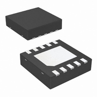
LP5996SDX-2533/NOPB National Semiconductor, LP5996SDX-2533/NOPB Datasheet - Page 11

LP5996SDX-2533/NOPB
Manufacturer Part Number
LP5996SDX-2533/NOPB
Description
IC REG 300/150MA RF/ANLG 10LLP
Manufacturer
National Semiconductor
Datasheet
1.LP5996SD-2828EV.pdf
(14 pages)
Specifications of LP5996SDX-2533/NOPB
Regulator Topology
Positive Fixed
Voltage - Output
2.5V, 3.3V
Voltage - Input
2 ~ 6 V
Voltage - Dropout (typical)
0.11V @ 150mA, 0.21V @ 300mA
Number Of Regulators
2
Current - Output
150mA (Min), 300mA (Min)
Operating Temperature
-40°C ~ 85°C
Mounting Type
Surface Mount
Package / Case
10-LLP
Lead Free Status / RoHS Status
Lead free / RoHS Compliant
Current - Limit (min)
-
Other names
LP5996SDX-2533
increase about 2:1 as the temperature goes from 25°C down
to -40°C, so some guard band must be allowed.
ENABLE CONTROL
The LP5996 features active high enable pins for each regu-
lator, EN1 and EN2, which turns the corresponding LDO off
when pulled low. The device outputs are enabled when the
enable pins are set to high. When not enabled the regulator
output is off and the device typically consumes 2nA.
If the application does not require the Enable switching fea-
ture, one or both enable pins should be tied to V
regulator output permanently on.
To ensure proper operation, the signal source used to drive
the enable inputs must be able to swing above and below the
specified turn-on/off voltage thresholds listed in the Electrical
Characteristics section under V
BYPASS CAPACITOR
The internal voltage reference circuit of the LP5996 is con-
nected to the C
external capacitor, connected to this pin, forms a low-pass
BYP
pin via a high value internal resistor. An
IL
and V
IH
.
IN
to keep the
11
filter which reduces the noise level on both outputs of the de-
vice. There is also some improvement in PSSR and line
transient performance. Internal circuitry ensures rapid charg-
ing of the C
ceramic capacitor with either NPO or COG dielectric is rec-
ommended due to their low leakage characteristics and low
noise performance.
SAFE AREA OF OPERATION
Due consideration should be given to operating conditions to
avoid excessive thermal dissipation of the LP5996 or trigger-
ing its thermal shutdown circuit. When both outputs are en-
abled, the total power dissipation will be P
where PD = (V
In general, device options which have a large difference in
output voltage will dissipate more power with both outputs
enabled, due to the input voltage required for the higher out-
put voltage LDO. In such cases, especially at elevated ambi-
ent temperature, it may not be possible to operate both
outputs at maximum current at the same time.
BYP
IN
capacitor during start-up. A 10nF, high quality
- V
OUT
) x I
OUT
for each LDO
D(LDO1)
www.national.com
+ P
D(LDO2)


